
Each year the IEEE Awards Board recommends a select group of recipients to receive IEEE’s most prestigious honors. These are individuals whose exceptional achievements and outstanding contributions have made a lasting impact on technology, society, and the engineering profession.
The 2024 IEEE Technical Field Award recipients listed below will receive their awards at 2024 IEEE-sponsored conferences.
To view a complete list of recipients in all years, select the past and present recipients link shown below. Once in the document, there will be links to each award that are clickable and you can view recipient citations as well.
The 2024 IEEE Medal and Recognition Recipients will receive their awards at the 2024 IEEE VIC Summit and Honors Ceremony on 3 May 2024 in Boston, Massachusetts, USA. Secure your registration NOW before it’s too late.
IEEE Medal of Honor
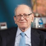
Robert E. Kahn
“For pioneering technical and leadership contributions in packet communication technologies and foundations of the Internet.”
IEEE Frances E. Allen Medal

David J. Kuck
“For pioneering work in vector and parallel computer architecture, software, and compilers that enables many performance-sensitive applications.”
IEEE Alexander Graham Bell Medal

Jennifer Rexford
“For contributions to Internet wide-area routing and software-defined networking.”
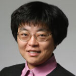
IEEE Mildred Dresselhaus Medal

Claire Tomlin
“For foundational work in the design and verification of cyber-physical systems with applications to safety in autonomous systems.”
IEEE Edison Medal
Vincent W. S. Chan
“For pioneering technical contributions and leadership in the fields of space and terrestrial optical communications and networks.”
IEEE Medal for Environmental and Safety Technologies

Hagit Messer
“For contributions to sensing of the environment using wireless communication networks.”
IEEE Founders Medal
Tsu-Jae King Liu
“For leadership in the advancement and commercialization of nanometer semiconductor technologies and the promotion of microelectronics workforce development.”
IEEE Richard W. Hamming Medal

Alexander Barg
“For contributions to the theory of error-correcting codes and their applications in distributed storage, non-volatile memory, and digital fingerprinting.”
IEEE Medal for Innovations in Healthcare Technology

Blake S. Wilson and Graeme Clark
“For contributions to the development of the modern cochlear implant.”
IEEE Medal for Innovations in Healthcare Technology
Graeme Clark and Blake S. Wilson
“For contributions to the development of the modern cochlear implant.”
IEEE Nick Holonyak, Jr. Medal for Semiconductor Optoelectronic Technologies
Constance J. Chang-Hasnain and Fumio Koyama
“For pioneering contributions to vertical-cavity surface-emitting laser (VCSEL) and VCSEL-based photonics for optical communications and sensing.”
IEEE Nick Holonyak, Jr. Medal for Semiconductor Optoelectronic Technologies
Fumio Koyama and Constance J. Chang-Hasnain
“For pioneering contributions to vertical-cavity surface-emitting laser (VCSEL) and VCSEL-based photonics for optical communications and sensing.”
IEEE Jack S. Kilby Signal Processing Medal
Palghat P. Vaidyanathan
“For contributions to multirate digital filter banks and sparse array signal processing.”
IEEE/RSE James Clerk Maxwell Medal
Kam Yin Lau
“For spearheading high-speed semiconductor lasers and RF-over-Fiber Systems, enabling today’s wireline and wireless broadband access.”
IEEE James H. Mulligan, Jr. Education Medal

Andrea J. Goldsmith
“For educating, mentoring, and inspiring generations of students, and for authoring pioneering textbooks in advanced digital communications.”
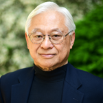
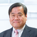
IEEE Jun-ichi Nishizawa Medal
John E. Bowers
“For contributions to photonic integrated circuit technologies.”
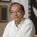
IEEE Robert N. Noyce Medal

MING-KAI, TSAI
“For vision and leadership in the global semiconductor industry, democratizing technology access for billions of people.”
IEEE Dennis J. Picard Medal for Radar Technologies and Applications
Fred Daum
“For research, design, development, analysis, and testing of complex phased array radar systems, making them work in the real world.”
IEEE Medal in Power Engineering
Deepak Divan
“For contributions to advanced power conversion technologies for modern electric power grids.”
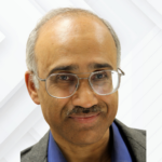
IEEE Simon Ramo Medal

John A. Stankovic
“For contributions to the theory of real-time and resource-constrained, distributed systems and the practice of cyber-physical and health systems.”
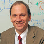
IEEE John von Neumann Medal

Christopher D. Manning
“For advances in computational representation and analysis of natural language.”
President’s Award
Gladys B. West
"For mathematical modeling and development of satellite geodesy models that played a pivotal role in the development of the Global Positioning System (GPS)."
IEEE Honorary Membership
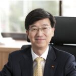
Sung Wook Park
“For contributions to expand the influence of technology and to improve the ecosystem of the global semiconductor industry.”
IEEE Corporate Innovation Award
AMD
“For leadership in development and deployment of chiplet architecture designs for high-performance and adaptive computing.”
IEEE Richard M. Emberson Award
Stefan Mozar
“For sustained contributions and leadership of multiple IEEE Societies and Technical Communities, and IEEE Conferences.”
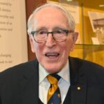
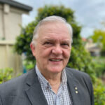
IEEE Haraden Pratt Award
Tariq S. Durrani
“For sustained leadership and outstanding contributions to the IEEE in education, technical activities, awards, and global connections.”
IEEE Theodore W. Hissey Outstanding Young Professional Award

Simay Akar
“For leadership and inspiration of young professionals with significant contributions in the technical fields of photovoltaics and sustainable energy storage.”
IEEE Eric Herz Outstanding Staff Member

Jamie Moesch, 2023 Recipient
“For exceptional leadership within IEEE Educational Activities and sustained and substantial contributions to the goals and objectives of IEEE.”
IEEE Biomedical Engineering Award

John A. Rogers
"For multi-disciplinary contributions in the life sciences, physical sciences, engineering, and medicine to enable the integration of biology and electronics.”
IEEE Cledo Brunetti Award

Adrian Mihai Ionescu
“For leadership and contributions to the field of energy-efficient steep slope devices and technologies.”
IEEE Control Systems Award
Alain Bensoussan
“For fundamental contributions to stochastic control, control-theoretic methods in management and finance, and impactful leadership of scientific and engineering organizations.”
IEEE Electromagnetics Award

Kamal Sarabandi
“For contributions to electromagnetic sensing technology and metamaterials for antenna miniaturization.”
IEEE James L. Flanagan Speech and Audio Processing Award

Keiichi Tokuda
“For pioneering contributions to statistical speech synthesis and speech signal processing.”
IEEE Fourier Award for Signal Processing

Stéphane G. Mallat
“For contributions to the theory and applications of wavelets and machine learning.”
IEEE Andrew S. Grove Award
Tsunenobu Kimoto
“For contributions to silicon carbide material and power devices.”
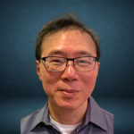
IEEE Herman Halperin Electric Transmission and Distribution Award
Joe Hong Chow
“For contributions to the modeling and control of large-scale power transmission systems.”
IEEE Masaru Ibuka Consumer Technology Award
Steve B. Furber and Sophie Wilson
“For the design of the 32-bit ARM RISC microprocessor.”
IEEE Masaru Ibuka Consumer Technology Award

Sophie Wilson and Steve B. Furber
“For the design of the 32-bit ARM RISC microprocessor.”
IEEE Internet Award

Walter Willinger
“For contributions towards a foundational understanding of Internet traffic and topology.”
IEEE Richard Harold Kaufmann Award
Giuseppe Buja
“For fundamental contributions to modulation and control of industrial drives.”
IEEE Joseph F. Keithley Award in Instrumentation and Measurement

Deepak G. Uttamchandani
“For contributions to photonics-based optical frequency and wavelength domain instrumentation and measurement.”
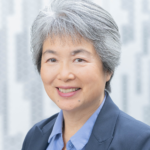
IEEE Gustav Robert Kirchhoff Award

Mary Jane Irwin
“For contributions to electronic design automation and power-aware computer architecture.”
IEEE Leon K. Kirchmayer Graduate Teaching Award
David N. Tse
“For inspirational mentoring and contributions to graduate teaching in wireless communication, power systems, computational biology, and blockchains.”
IEEE Koji Kobayashi Computers and Communications Award

Anja Feldmann
“For contributions to the field of networking and Internet technologies, specifically to traffic engineering, network measurements, and Internet protocols.”
IEEE William E. Newell Power Electronics Award
David J. Perreault
“For contributions to the development of very-high-frequency power converters.”
IEEE Donald O. Pederson Award in Solid-State Circuits

Deog-Kyoon Jeong
“For leadership in the technology development for Digital Video Interface (DVI) and High-Definition Multimedia Interface (HDMI).”
IEEE Frederik Philips Award

Bich-Yen Nguyen
“For leadership in the research, development, and commercialization of innovative silicon-on-insulator substrates, process technologies, and devices.”
IEEE Photonics Award

Kim Roberts
“For leadership in the introduction and development of digital coherent signal processing for optical fiber transmission systems.”
IEEE Robotics and Automation Award
Paolo Dario
“For establishing and advancing bionics and biorobotics as key research areas worldwide, integrating robotics and medicine.”
IEEE Frank Rosenblatt Award

Bernadette Bouchon-Meunier
“For contributions to the foundations and applications of approximate reasoning and fuzzy systems.”
IEEE Marie Skłodowska-Curie Award

Richard E. Carson
“For contributions to image reconstruction and tracer kinetic analysis in positron emission tomography.”
IEEE Innovation in Societal Infrastructure Award

Elena Ferrari
“For pioneering and sustained contributions to the security and privacy of online social networks.”
IEEE Charles Proteus Steinmetz Award

Gary R. Hoffman
“For leadership in and development of power systems standards to increase global adoption.”
IEEE Eric E. Sumner Award
Stephen B. Weinstein, Leonard J. Cimini, Jr., and Geoffrey Ye Li
“For fundamental contributions to frequency domain communications including orthogonal frequency division multiplexing.”
IEEE Eric E. Sumner Award
Leonard J. Cimini, Jr., Geoffrey Ye Li, and Stephen B. Weinstein
“For fundamental contributions to frequency domain communications including orthogonal frequency division multiplexing.”
IEEE Eric E. Sumner Award
Geoffrey Ye Li, Stephen B. Weinstein, and Leonard J. Cimini, Jr.
“For fundamental contributions to frequency domain communications including orthogonal frequency division multiplexing.”
IEEE Nikola Tesla Award

Aldo Boglietti
“For contributions to the magnetic and thermal modeling, design, and characterization of electrical machines.”
IEEE Kiyo Tomiyasu Award
Davide Scaramuzza
“For contributions to agile visual navigation of micro drones and low-latency robust perception with event cameras.”
IEEE Rao R. Tummala Electronics Packaging Award
Madhavan Swaminathan
“For contributions to semiconductor packaging and system integration technologies that improve the performance, efficiency, and capabilities of electronic systems.”
IEEE Transportation Technologies Award

V. Anand Sankaran
“For contributions to the advancement and high-volume implementation of automotive electrification technologies.”
IEEE Undergraduate Teaching Award

R. Iris Bahar
“For innovative undergraduate teaching and transformative student mentoring that champion inclusivity in engineering and examine societal impacts of technology.”
IEEE Lotfi A. Zadeh Award for Emerging Technologies

Andras Kis
“For pioneering work and breakthroughs on 2D materials and electronic devices.”