Technical Briefs
Marvels in Microelectronic Devices Structure: Actuate, Isolate and Interconnect
by Simon Deleonibus, Past Chief Scientist, CEA,LETI
Looking for the Holy Grail device having the lowest parasitics, the highest performance and the lowest leakage current has been the rule of the game for microelectronics since Large Scale Integration (LSI) offered the possibility to design complex circuits for digital and mixed signals applications. In their time, groundbreaking ideas to actuate, isolate and interconnect all devices with the smallest footprint possible have been proposed. Among these, channel/substrate engineering with Silicon on Insulator (SOI), Local Oxidation of Silicon (LOCOS) and Shallow Trench Isolation (STI), and copper interconnects have been developed worldwide, as breakthroughs in high risk/high gain projects pushed by highly talented teams and their charismatic leaders.
The attractiveness of SOI was put forward for its unbeatable isolation capabilities and low junction capacitance, especially for power, radio frequency or rad-hard applications. Initially considered as restricted to niche applications, SOI is nowadays considered a mainstream substrate, a must for RF and Low Power applications and is a candidate to replace bulk Si in the high performance market.
SOI was first mentioned in the 1960s during the search of epitaxially grown Silicon on Sapphire (SOS), which was supposed to “almost“ epitaxially match perfectly with Si (100). The “almost” was actually a best case 7% crystallographic strain mismatch, thus thermal mismatches, between Si and sapphire induced a substantial number of crystallographic defects, such as threading dislocations (106–107/cm2) [1]. The first demonstration of SOS was made in 1968 by HM Manasevit and WI.I. Simpson at North American Aviation, Inc., later on known as North American Rockwell Corp. [2], [3]. Following a decomposition of SiCl4 by H2 at 1250 °C, the substrate was reduced by Si. Further coalescence of the reacting Si atoms occurred on the surface of alpha alumina.
Jean Pierre Colinge, 2012 IEEE A. Grove Award recipient, now with CEA, LETI, reports: “In the early 1980's, the only proven SOI technology was SOS (Silicon on Sapphire), which was used in military/aerospace applications because of its resistance to radiation, and in some Hewlett-Packard computers, the 1000 Series processor in the L-Series computers introduced in 1979 [6]. SOS technology was, however, clearly unsuitable for 3D monolithic integration, and other techniques, based on laser/lamp melting and recrystallization or various epitaxial techniques, were developed.” From the late 1970s to the beginning 1990s, various alternatives to SOS were developed on full sheet substrates (BESOI by IBM in the 1970s; ELTRAN by Canon in 1990) or by 3D process integration (Zone Melted Recrystallization ZMR since the 1980s). “The real breakthroughs in SOI wafer fabrication were the Separation by Oxygen Implantation (SIMOX) technique, first used in 1978 to fabricate CMOS circuits by NTT [4], and the Smart-Cut process, invented by LETI [5], [7].” SIMOX kept on improving by perfecting substrate annealing during oxygen implantation and high temperature annealing (by CEA,LETI at 1300 °C) [8], multi-implantation (by Monsanto) [9] and low energy implantation (by Spire) [10]. Defect density drastically dropped by 4 orders of magnitude (102–103/cm2) compared to SOS.
Since the late 1960s, Michel Bruel, was involved at CEA, LETI to develop defect free heavy dose ion implantation. With his team and the collaboration of visiting Professor Stoemenos, of Thessaloniki University, he was the right person to successfully address the reduction of defect density in SIMOX, which he succeeded in, and finally he invented SMARTCUT. Michel Bruel says: “I wanted to imagine new solutions better suited than SIMOX for electronic mass market applications. I thought of a fracturing process, based upon defects generated at their projected end of range (Rp) by light ions implanted at high dose, giving rise to the formation of nano-gaseous bubbles and nano-fracturing. Hydrogen, or helium gas ions, would penetrate into silicon without introducing any damage along the major part of the Rp. By tuning the acceleration voltage on the implanter, we could choose the depth of the nano fracturation layer, i.e. the thickness of the layer to be created. After the implant, we bonded the substrate to a handle wafer, applied a thermal cycle that fractured the implanted substrate. We removed the initial substrate before smoothly polishing the final SOI substrate surface. The initially fractured wafer was recyclable. This process was directly applicable in a microelectronics environment. We wanted to keep some lead time: the invention was kept confidential from 1991 to 1995.” Meanwhile, SIMOX was used to process radiation hardened high speed microprocessors of the 68000 family, for military and space applications, as soon as 1988. Michel Bruel received many awards for the invention of the SMARTCUT process, among which was the 2008 IEEE Cledo Brunetti Award. In 1992, in the context of the fall of Berlin wall, André-Jacques Auberton-Hervé and Jean-Michel Lamure started SOITEC, with the support of Michel Bruel in the clean rooms of CEA, LETI, and were convinced to apply the technology to future low power and high performance civilian applications. Initially a company of 4 employees, today SOITEC counts 1000 employees worldwide. SOITEC has ramped up the SMARTCUT wafer production since 1993 and is nowadays the provider of 90% of the SOI market worldwide. Auberton-Hervé, SOITEC CEO until 2015, declares: “We licensed SEH in 1997 and used the money to invest in our first factory. Nobody believed we could challenge them not only on innovation but also on production.” SMARTCUT SOI wafers have a diameter range from 50 to 450 mm, with the lowest defect density, comparable to what is provided on commercial bulk silicon by volume. The SMARTCUT principle is applied to many different materials that could be bonded to an oxidized Si wafer.
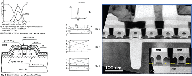
(left ) The first SIMOX paper [4]. (middle) Smartcut principle: European patent EP/FR9111491, filed Sept. 18, 1991 by Michel Bruel (CEA, LETI)[5] showing the 3 major steps of ion implant into the substrate through a screening layer, bonding to a handle wafer and splitting of the new substrate at the fracture zone around Rp after heat treatment. (right) Ultra thin FD devices for CMOS scaled logic applications.(Tsi = 6 nm TBOx = 20 nm) Lg = 14 nm processed on 300 mm SMARTCUT wafers (middle and right figures provided by courtesy of CEA, LETI)
Ghavam Shahidi, the IEEE 2010 Cledo Brunetti and 2006 JJEbers Awards recipient, was among those who pioneered the realization of VLSI designs on Partially Depleted SOI as soon as 1989 at IBM. Shahidi says: “Over the first 10 years, the biggest ‘non-technical’ challenges were convincing the IBM management and end users to commit product to SOI technology.” It took 8 years in device engineering and development to achieve the first complex circuit demonstration (the Power PC601). The “first commercial IBM's Power 4 processor in 180 nm CMOS SOI technology, came out in 2001, first IBM's giga frequency processor and largest chip at the time.” Other companies adopted partially depleted SOI in the 180 down to 45 nm nodes, such as Freescale (Power PC7455 CPU), AMD (K series) or SONY (Xbox360, PS3, Wii).
Fully depleted and multigate/ Gate-All-Around architectures have been studied since the 1980s by SONY [11], CEA,LETI [12], Hewlett-Packard [13], IMEC [14] and are necessary to reach a MOSFET minimum subthreshold slope of 60 mV/dec, and thus reduce drastically leakage current. The reduction of Si (TSi) and buried oxide (BOx) thicknesses are the prime challenges to scaledown CMOS devices. It took approximately ten years to achieve sub-20 nm gate lengths devices on less than 10 nm thin SOI and 10 nm thin BOx on 300 mm wafers [15]. OKI was the first company to ship in 2000 an ultra low power circuits based on FDSOI, including an MCU, power circuits, memory and LCD driver. STMicroelectronics, IBM and Globalfoundries adopted FDSOI for their sub-28 nm nodes, moving towards 10 nm. As such, SMARTCUT is a desirable choice for monolithic 3D integration based on thin film devices [16].
Beyond digital applications, SOI is fulfilling the promise of penetrating the More-Than-Moore diversification market. SMARTCUT is providing 90% of the RF Front-End devices for mobile phones. The substrate engineering has been refined by including high resistivity and a trap rich interface at the buried oxide backside [17], [18] to enhance the final apparent substrate resistivity and, thus, reduce the cross talk to the substrate significantly. Many teams worldwide such as IBM and CEA, LETI/STMicroelectronics, have been developing the integration of RF and mixed signal technology on SOI since the early 2000s. The exceptional vertical isolation and high quality passivation brought by such a thick oxide, combined to high resistivity silicon and trap rich oxide backside interface, makes it ideal to enable co-integrated RF switches with LNA [19], [20]. Auberton-Hervé concludes: “In the past 3 decades, SOI has also been the test bench for Si based diversification for sensors, photonics systems, on-chip applications for communication and data transmission, and concentration PV system markets. It is still able to expand to other areas.”
Lateral field isolation is
The introduction of LOCOS needed new process alternatives. LOCOS isolation posed new constraints at the integration level: knowledge on selective oxidation, nitride selective etching, stress induced in the active area during oxidation, generation of stacking faults or dislocations depending on the oxidation conditions, nitridation of active area edge (Kooi effect), etc. The fact that the silicon nitride oxidation rate is much less than Si’s (under 1 atm it is several 10x higher), is a remarkable property that was advantageously exploited by E. Kooi and his team (1966 patent [23]) and published in 1969 and 1970 [21]. The initial motivation to introduce LOCOS isolation was to reduce the lateral diffusion of dopants that reduced the distance between active areas and increased the lateral parasitic capacitance of p-n junctions in planar technology. That, of course, had great impact on bipolar devices too and could be extended to MOSFET technology. Marc J. de Vries and Kees Boersma reported in 2005 [24]: “All this happened in connection with MOS (Metal Oxide Semiconductor) ICs…it was quite some time before the Nat. Lab. was prepared not only to work on bipolar ICs for analogue purposes, but also to work on MOS, which was considered to be more suitable for digital techniques.”
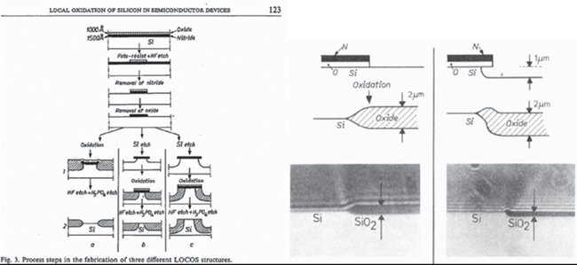
(left) LOCOS isolation invented by Appels and Kooi, first presented at 3rd Conference Solid State Devices in 1969 at Exeter(UK) [21]: three options for process flow showing the selective oxidation of silicon and increasing recess of field oxide. No pad oxide was used (right) LOCOS isolation: semirecessed and recessed [22]. A pad oxide is used to reduce dislocations. The bird’s beak and bird’s head appear on the semirecessed and recessed versions respectively. (by permission of Koninklijke Phillips Electronics N.V.)
A dopant free lateral recessed isolation was needed. The solution they imagined was to recess an insulator (silicon dioxide) because the direct moat isolation was degrading the step coverage problem (gate metallization and lithography), without stopping the diffusion of dopants. LOCOS isolation, in spite of the bird’s beak introducing a feature size loss, was an elegant solution at the introduction of polysilicon gate. For decades, major teams worldwide have been working on a huge number of solutions to reduce the bird’s beak, to planarize and reduce strain at the active area edge. These solutions were rich of imaginative constructions named SWAMI (Sidewall Masked Isolation), Poly Buffer LOCOS, SILO (Sealed Interface Local Oxidation of Silicon), SuperSILO, FuROX, etc., aiming at a bird’s beak reduction and planarization of the topography with extra process costs as compared to the initial process. The whole microelectronics business has been using them intensively until the early 2000s, and still adopt them for specific solutions in the More-Than-Moore diversification domain. None of the modified LOCOS solutions could totally suppress the Kooi effect (the so called “white ribbon”), because the combined use of silicon nitride and steam oxidation inherently causes it. A sacrificial oxidation removes the nitrided silicon at the active area edge and allows the growth of a reliable non-thinned gate oxide. Kooi and Appels proposed very quickly (in 1970) to adopt such a solution to eliminate the Kooi effect.
Only SILO could prove zero bird’s beak compatible with zero defect provided that a thin nitride (10 nm) was sealed to the active area by 1 nm Rapid Thermal Nitridation (RTN) [26], [27] or later on by a transfer under vacuum in the LPCVD reactor. The ultimate scaling limits of LOCOS type isolation schemes came from the field oxide thinning and 2-dimensional (2D) increase in bird’s beak value appearing in small geometries. SuperSILO brought a drastic reduction of the bird’s beak and of the 2D effects down to 100 nm active area width [27]. Meanwhile, STI was making progress thanks to Chemical Mechanical Polishing (CMP) planarization.
From the early 1980s, various approaches to achieve a workable STI were carried out in the semiconductor companies worldwide (such as Toshiba, [28]) using a non-selective etchback of a thin resist and deposited oxide bilayer. This technique suffered from uniformity issues and residues due to slight deviations from 1/1 selectivity etching. Bijan Davari, IBM, declares: “I realized the potential of STI around 1985 for both logic and memory applications. This included all the CMOS technologies for both High-performance and Low-power applications and standalone DRAM.” The most important hurdle for STI was the planarization for variable pattern factor isolation structures. The planarization problem resulted in too much “dishing” in large isolation areas and not adequate removal of the deposited field insulator in small isolation areas.
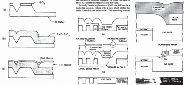
(left) STI by using sacrificial deposited oxide and several resists by Shibata et al. at 1982 IEDM [28]; (right) Planarization by block resist and etch back to alleviate the dishing problem was published by Davari et al. at 1988 IEDM [29]; CMP was added later in 1989 to obtain full planarization.
Besides the optimization of gate insulator breakdown, junction leakage (areal and peripheral) and field doping, a large number of CMP techniques (see also January 2019 Newsletter issue), were tested for the very first time in the FEOL process. Bijan continues: “We achieved a breakthrough around 1988 by demonstrating a perfectly planar STI process for a very demanding variable pattern factor 16Mb DRAM technology at IBM. This was achieved by a combination of chemical-mechanical polishing (CMP) and reactive-ion-etching (RIE) with dummy patterns that were generated prior to RIE by an automated placement algorithm based on the pattern factors of the underlying isolation and the adjacent structures. We created the design tools for the pattern generation that was subsequently used in all our products [30]. The STI technology then became the industry standard for device isolation. It took us about 3 years to go from test site, single device isolation experiments to fully functional circuits, and then another 2 years to product. Our first product was a 16 Mb DRAM with STI and deep trench for storage capacitance.” Davari was the IEEE 2005-JJ.Ebers and 2010 A. Grove Awards recipient.
Geometric downscaling revealed limitations in materials properties such as aluminum: another major breakthrough was needed for interconnects. The introduction of copper (Cu) on-chip multilevel interconnects (BEOL, back end of line) took a long path since the 1980’s, when the limitations of aluminum (Al) wiring at smaller geometries due to scaling started to appear. The first attempt to solve scaling issues concentrated on the flattening of topography while keeping Al for metal wiring. In strong synergy with the efforts carried out on STI (hereabove), CMP was introduced by IBM in 1991 to planarize interlevel dielectrics (ILDs) on pre-etched metal lines, and to polish separate interlevel studs, or “vias” made of tungsten [30]. The obtained planarization enabled stacking of multiple wiring levels at constant minimum pitch, and improved lithographic patterning.
Important efforts were carried out to keep the conventional subtractive-etched/ILD backfill scheme to introduce Cu metallization. Its higher reflectivity pushed towards hard-mask lithography and perfect planarization of topography. The absence of volatile Cu etching byproducts at room temperature required etching temperatures higher than 200 °C (at 250 °C: by NTT [31], or at 220 °C by Rensselaer Institute [32]). The passivation of Cu lines was very critical and requested anti-corrosion treatments included in the etching steps. Further, since Cu ions can diffuse rapidly through SiO2 dielectric, and can potentially poison Si devices, each Cu wire had to be encapsulated by a diffusion barrier. This requirement would have been quite difficult for subtractively-etched Cu lines, with their exposed and reacted sidewalls and top surfaces. These Cu etching difficulties coupled with the need for high-performing planarization pushed towards a different paradigm. That was the Damascene or Dual Damascene scheme with its ILD patterning, conformal metal fill, and excess metal CMP developped by IBM (see figure, Newsletter january 2019 issue and [33], [34]). Dual damascene had been introduced earlier for DRAM W interconnects [30], and emerged for Cu (VMIC 1993) [35]. Finally, IBM discovered that by modifying the recipe for electrolytic Cu plating used for packaging interconnects, they could fill high aspect-ratio lines and vias with no voids or seams, with a “superfilling” plating process that improved as the wires got narrower. It produced a quantum leap improvement in electromigration reliability (assuming integration with a proper diffusion barrier). This winning combination has kept the door open for Moore’s Law BEOL scaling, extending Cu BEOL for over 20 years and 9 generations in manufacturing [35].
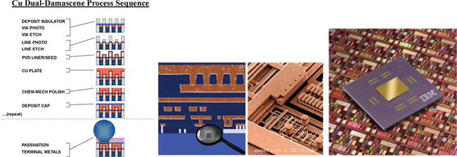
(Left )double damascene schematic process flow; (right) Publicity photos from CMOS/Cu BEOL technology announcement, showing 6-level Cu dual damascene wiring, and world’s first Cu BEOL production chip (PPC750) [35] (D.Edelstein by courtesy).
Dan Edelstein, IBM, says: “In the mid 1980’s, IBM started the initial drive to migrate from Al(Cu) to Cu/low-k BEOL, initiated by my colleague C-K Hu, to meet our growing needs for bipolar-based mainframe CPU high-current circuits (with high EM reliability). In the early 1990’s, the needs switched to low-parasitic capacitance, higher-density and lower-cost CMOS wiring.” Edelstein adds: “Besides matched CTEs and high modulus for SiO2 ILD vs. passivation, I had found in the literature that SiO2 possessed a very low Cu solubility limit, despite the high diffusivity of Cu atoms, and OH-catalyzed Cu ionization in BEOL-level electric fields leading to much faster Cu ion drift diffusion.”
The team had to respond the fundamental questions of deposition, patterning and containing the interconnect material. “The retained options were: 1) PVD Cu seed + damascene (superfilling) electrolytic plating, 2) (Dual) Damascene dielectric patterning with 2-step CMP of Cu/barrier, or 3) Full encapsulation of Cu lines and vias with diffusion barriers of TaN/Ta bilayer liner plus Si3N4 dielectric cap. The combination of these barriers with SiO2 interlevel dielectric, plus the additional Si3N4 barriers between FEOL and BEOL provided redundant protection against Cu corrosion, migration, interline leakages, and FEOL device poisoning.”
The first functional microprocessor product was demonstrated in Q4 1997, as early-user hardware, on a 0.22 µm production high-performance CPU chip (PowerPC 750 for Apple). It took approximately 3/4 year to qualify this for high-volume production. “The much less mature Cu technology demonstrated the expected frequency improvement (ISSCC 1998) [35], and had tighter clock skew distributions, electromigration lifetimes and statistics way beyond the spec limit.” During the past two decades, the SiOx dielectric has evolved by doping and density reduction into SiOF, SiCOH with low k SiCN(H) caps, and ultralow-k porous SiCOH (IEDM 1999 and 2006, IITC 2004) [35]. Copper/airgap for 2 fatline levels was introduced into manufacturing by Intel in 14 nm [36]. For the sub-10 nm nodes, Co or Ru wiring for the finest BEOL levels, or Cu encapsulation by Co, were envisaged (already presented by Komatsu at MRS MAM 2007) to limit/suppress electromigration [35], [37], in spite of higher Co and Ru resistivities that might be recovered for 7 nm barrierless Cu lines. D. Edelstein, A. Grill and C-K Hu are the 2019 Cledo Brunetti Award recipients for their contribution to Cu/Low K technology.
References
[1] J.-P. Colinge, in “Silicon-On-Insulator Technology: Materials To VLSI”, The Kluwer international series in engineering and computer science, Kluwer Academic Publishers, New York (1991), DOI 10.1007/978-1-4757-2121-8.
[2] H.M. Manasevit and W.I. Simpson, “Single-Crystal Silicon on a Sapphire Substrate”, J. Appl. Phys. 35, 1349 (1964)
[3] H.M. Manasevit and W.I. Simpson, “Epitaxial deposition of silicon on alpha-aluminum”, US patent 379,668, filed July 1, 1964.
[4] K. Izumi, M. Doken, H. Ariyoshi, “CMOS devices fabricated on buried SiO2 layers formed by oxygen implantation into silicon”, Electronics Letters, vol.14, n°18, pp593–594 (1978)
[5] M.Bruel, “Procédé de fabrication de films minces de matériau semiconducteur”, European patent EP/FR9111491, filed Sept. 18, 1991
[6] http://www.hpmuseum.net/exhibit.php?class=3&cat=37
[7] M. Bruel, “Silicon on insulator material technology”, Electronics Letters, vol. 31, N°14, pp.1201–1202, (1995)
[8] J. Stoemenos, C. Jaussaud, M. Bruel, and J. Margail, “New conditions for synthesizing SOI structures by high dose oxygen implantation”, J. Crystal Growth, Vol. 73, p.546, 1985
[9] D. Hill, P. Fraundorf and G. Fraundorf, Proc. IEEE SOS/SOI Workshop, p. 29, 1987
[10] F. Namavar, E. Cortesi, B. Buchanan, and P. Sioshansi, Proc. IEEE SOS/SOI Workshop, p. 117, (1989)
[11] T. Sekigawa and Y. Hayashi, “Calculated threshold-voltage characteristics of an XMOS transistor having an additional bottom gate,” Solid-State Electronics. vol. 27, p. 827, 1984.
[12] A.J. Auberton-Herve, J.P. Joly, P. Jeuch, J. Gautier and J.M. Hode, “Device performances of a submicron SOI technology”, IEDM Tech. Dig., p. 808–811 (1984).
[13] J.-P. Colinge, “Transconductance of Silicon-On-Insulator (SOI) MOSFET’s”, IEEE Electron Devices Letters, vol. EDL-6, n°11, p. 573–574 (1985).
[14] J.-P. Colinge, M.H. Gao, A. Romano, H. Maes, and C. Claeys, “Silicon-on-insulator gate-all-around device”, IEDM Tech. Dig., pp. 595–598 (1990)
[15] V. Barral, T. Poiroux, F. Andrieu et al.,”Experimental investigation on the scalability of the strained FDSOI CMOS technology down to 2.5nm film thickness and 18nm gate length with a TiN/HfO2 gate stack”, IEDM Tech. Dig., pp. 61–64 (2007)
[16] P. Batude, M. Vinet, A. Pouydebasque et al., “Advances in 3D CMOS Sequential Integration”, IEDM Tech. Dig., pp. 345–348 (2009)
[17] D.Lederer, J.-P. Raskin, “Method of Manufacturing a Multilayer Semiconductor Structure with Reduced Ohmic Losses” patent no. FR0311347, filed September 26, 2003
[18] D. Lederer and J.-P. Raskin, “New Substrate Passivation Method Dedicated to HR SOI Wafer Fabrication With Increased Substrate Resistivity” IEEE Electron Device Letters, vol. 26,No. 11, Nov. 2005, pp. 805–807.
[19] F. Gianesello, D. Gloria, C. Raynaud, S. Montusclat et al., “Integrated Inductors in HR SOI CMOS technologies: on the economic advantage of SOI technologies for the integration of RF applications”, Proc. IEEE SOI Conf., pp 103–104, Indian Wells(CA), Oct 1–4, 2007.
[20] C. Raynaud, “Technology pathfinders for low cost and highly integrated RF Front End Modules”, IEDM Tech. Dig.,pp 466–469, San Francisco(CA), Dec. 15–17, (2014).
[21] J.-A. Appels and E. Kooi, 3rd Conference on Solid State Devices, Exeter (UK) (1969) and also J.-A. Appels, E. Kooi, M. M. Paffen et al., “Local oxidation of silicon and its application in semiconductor device technology”, Philips Res. Repts 25, pp. 118–132, (1970)
[22] J-A Appels and Pfaffen, “Local Oxidation of Silicon; new technological aspects”, Philips Res Repts 26, pp.157–165, June 1971
[23] E. Kooi, Patent # NL6614016A filed on October 5, 1966
[24] Marc J. de Vries and Kees Boersma, “80 years of Research at Philips Nat. Lab” Pallas Publications, Amsterdam (NL) (2005)
[26] S Deleonibus,P.Molle,J.Lajzerowicz et al., “High Performance Submicron SILO Process for High Density EPROM Memories Using Rapid Thermal Nitridation of Silicon”, Proc. ESSDERC, pp. 152–155, Berlin(FRG) (1989)
[27] S.Deleonibus, “A GIGABIT scalable SILO field isolation using Rapid Thermal Nitridation (RTN) of silicon”, Proc ESSDERC, pp. 75–78, Leuven(Be) (1992).
[28] T. Shibata, R. Nakayama, K. Kurosawa et al., “A Simplified BOx (Buried-Oxide) Isolation Technology for Megabit Dynamic Memories”, IEDM Tech. Dig., pp.27–30, San Francisco (CA)(1982)
[29] B. Davari, C.Koburger, T.Furukawa et al., “A variable-size shallow trench isolation (STI) technology with diffused sidewall doping for submicron CMOS”, IEDM Tech. Dig., pp. 92–95, San Fransisco(CA)(1988)
[30] Carter W. Kaanta, Susan G. Bombardier et al., “Dual Damascene: a ULSI Wiring Technology”, Proc. VMIC, pp144–152, Santa Clara(CA) (1991)
[31] Kazuhide Ohno, Masaaki Sato and Yoshinobu Arita, “High Rate Reactive lon Etching of Copper Films in SiCI4, N2, Cl2 and NHr Mixture”, Ext. Abs. SDDM Conf., pp. 215–218, Sendai(Japan)(1990).
[32] Howard, B.J. and Steinbruchei, Ch., Reactive Ion Etching of Copper with BC13 and SiCl4: Plasma Diagnostics and Patterning, J. Vac. Sci. Technol., A, 1994, vol. 12, no. 4, pp. 1259–1264.
[33] M.Chow, J.E. Cronin, W.L. Guthrie et al., US patent n° 4,789,648 (1988)
[34] K.Beyer, W.L. Guthrie, S.R. Makarewicz et al., US patent n° 4, 944, 836 (1990)
[35] a set of references can be found in: Daniel C. Edelstein, “20 Years of Cu BEOL in Manufacturing, and its Future Prospects”, IEDM Tech. Dig., pp. 334–337, San Francisco(CA)(2017)
[36] S. Natarajan, M. Agostinelli, S. Akbar et al., “A 14nm Logic Technology Featuring 2nd Generation FinFET Transistors, Air-Gapped Interconnects, Self-Aligned Double Patterning and a 0.0588 µm2 SRAM cell size”, IEDM Tech. Dig., pp.71–74, San Francisco(CA) (2014).
[37] C. Auth, A. Aliyarukunju, M. Asoro et al., “A 10nm high performance and low-power CMOS technology featuring 3rd generation FinFET transistors, Self-Aligned Quad Patterning, contact over active gate and cobalt local interconnects”, IEDM Tech. Dig., pp. 673–676, San Francisco(CA) (2017)
Save the Date!
EDS Governance Meeting Series
25-26 May 2019
Tarragona, Spain