Technical Briefs
Marvels of Microelectronic
Technology: from the Floating
Gate and Charge Trapping
concepts to the Flash Memory
of Terabit Class
by Simon Deleonibus, Past Chief Scientist CEA, LETI
Introduction
In this Technical Brief, we are focusing on the discovery, inventions and development of modern Non Volatile Memories (NVMs). Whereas, we reported on the invention and development of Dynamic Random-Access Memory (DRAM) in the October 2019 Newsletter issue.
Since the years 1990s to 2000s, NVMs, in their Flash Floating Gate and Charge Trap (FFG&CT) versions, have become the market and technology driver for integrated circuits as they entered the mass market through the camera, automotive and, further on, communication markets. Who among us has not used a USB key, a Solid State Disk (SSD), stored data on a mobile phone, or used a digital camera? No one can ignore today the formidable expansion of FFG&CT NVMs and the way they overcame the leadership on DRAM and Logic circuits as technology driver for Nanoelectronics. NVMs have gone through the highest number of conceptual and architectural changes in the past 50 years, evolving at the same time, from a niche product to a mass production driver. Just to give an example, Multi-Deca Gigabit (several tens of Gbit) USB keys, based on FFG&CT organized in a NAND architecture, are given almost for free nowadays as a storage and code share vector. Whereas, 256k NOR Erasable Programmable Read-Only Memory (EPROM), which were necessarily erased by using a UV lamp, were used for professional applications, essentially for storing microcontroller programs in the 1980s! Many hurdles have appeared in their 2-dimensional (2D) scaling, and today 3-dimensional (3D) multilevel cells (up to 4bits/cell) integration can increase the bit density without requesting conventional device scaling. The NAND FFG&CT memories have reached the Terabit integration level, using either an intermediate floating gate or pseudo floating gate charge trapping. Their market exceeded $52B in 2018, which is unprecedented. They are on the way to replacing hard disk drives (HDDs) in computers and equipping data centers with Solid State Disks (SSDs).
Two major key persons that marked the history of Non Volatile Memories research and development, Professor Simon M. Sze, NCTU, IEEE Fellow, IEEE EDS Celebrated member (Figure 1a) and Professor Fujio Masuoka, Tohoku University, IEEE Fellow (Figure 1b), have kindly accepted to testify on the birth of the discovery of the floating gate effect and the invention of Flash Memories, respectively. Their testimonies are reported in sections 1 and 2. In section 4, members of the former team at Toshiba Memory (spun into Kioxia) who invented and first announced the 3D BICS-FLASH3 architecture graciously accepted to share their recollection.
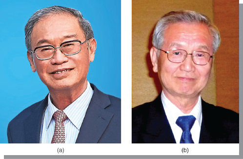
Figure 1 Recent portraits of: (a) Simon M. Sze (by courtesy of Simon Sze) (b) Fujio Masuoka (by courtesy of Fujio Masuoka)
1. Simon Sze and the early cradle age of Floating Gate memories
Everybody in the semiconductor business knows Professor Simon Sze for his very popular and authoritative books, discoveries and inventions. The author of this Technical Brief accompanied his learning of semiconductor devices as an undergraduate student through Simon Sze’s book titled Physics of Semiconductor Devices [1], first published in 1969, and is still using it daily as a reference just as many other scientists and engineers worldwide. Among the many seminal discoveries, inventions, studies and papers that Simon Sze authored in his career, the co-discovery of the Floating Gate Memory effect has certainly brought a revolution in our business and changed the societal way of living worldwide. Dawon Kahng and Simon Sze, Bell Labs researchers at that time, published a seminal paper in the Bell System Technical Journal in June 1967, in which they explained the Floating Gate Memory (FGM) effect [2]. The device featured a 50 Å SiO2 gate oxide, 1000 Å Zr floating gate, 1000 Å ZrO2 coupling insulator and an Aluminum control gate. Pulses at 50 V and 0.5 µs were necessary to inject charge through the gate oxide from the Insulated Gate Field Effect Transistor (IGFET) channel into the floating gate, by capacitive coupling between the control gate and the floating gate (Figure 2a). Depending on the insulator, the charge injection (Figure 2b) was believed to be due to a Fowler-Nordheim (for example in SiO2 or Al2O3) or Poole-Frenkel (Si3N4) mechanisms.
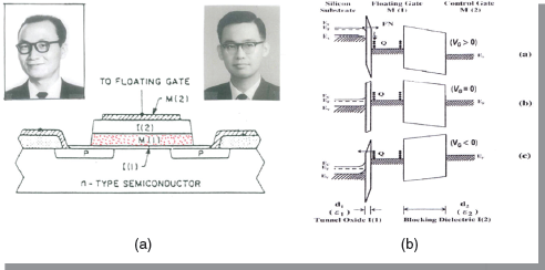
Figure 2(a) First floating-gate memory (FGM) by Dawon Khang (left) and Simon Sze (right). (Courtesy of Simon Sze) and Figure 2(b) Band diagram of a Floating gate transistor structure during: (a) charge trapping,(b) storage and (c) detrapping (discharging) (Courtesy of Simon Sze)
This was the very beginning of 60 years in research and development on the basic principle of charge storage/trapping in a stacked gate (1 control gate and 1 floating gate) device, and neutralization of the charge by an erasure mechanism, for example by applying an opposite voltage on the control gate. Without naming it explicitly, Kahng and Sze believed that such a device was announcing the Electrically Erasable Programmable Read-Only Memory (EEPROM). Many options and many divergent interests existed around the table without a dominant application really emerging at the beginning.
Since then, the Floating gate memory cell has proven to be the smallest memory device based on one transistor. It has beaten all predictions after being unrecognized or criticized as being expensive to make, unreliable and incompatible with logic devices, due to high program/erase voltages, and thus necessarily using a thick gate oxide susceptible to being stressed and suffering from induced defects. Nowadays, on the contrary, it has become a commodity product offering programmable/erasable mass storage media after 50 years of continuous struggle and studies.
In the frame of our exchanges, Prof. Simon Sze explained the motivations that led him and D. Kahng to invent the floating gate device for memory applications: “In the mid 1960’s, magnetic core memory (MCM) was used in computers. It took a long time to turn on the mainframe computer (m/c). We thought a semiconductor memory should be faster than the MCMs to boot up the mainframe computer (m/c).” Simon Sze adds: “When we submitted our paper to BSTJ in May 1967, we really did not know that FGM would eventually supersede all prior non-volatile memory technologies (e.g. magnetic tapes, HDDs, optical disks) and in early 21st century ushered in the 4th Industrial Revolution and brought unprecedented benefit to the mankind.” The paper introduced not only the basic concept of non-volatility in semiconductor devices, but also the floating-gate structure which is still the dominant technology for nonvolatile information storage.
In those days, many engineers and researchers wanted to use Read Only Memories for code storage by an electrical action, without necessarily being able to erase and program again. That is why the devices were pointed out as “alterable memories”. Coincidentally with Kahng and Sze’s discovery, in December 1967, H.A.R. Wegener from Sperry Rand Research Center published research on the Metal, Nitride Oxide Silicon (MNOS) transistor [3] in which charges were stored in silicon nitride layer traps by the Poole-Frenkel transport, after injection through the underlying tunnel oxide (Figure 3a). It resulted in a memory device with low charge retention capabilities, due to leakage through the gate. Other authors reported similar structures [4]. Keshavan and Lin reported on the band gap engineering of the insulating stack by introducing an extra oxide layer between the gate and channel, resulting in a MONOS structure [5]. The extra layer avoided charge leakage from the nitride to the gate and modified the transistor threshold voltage as well.
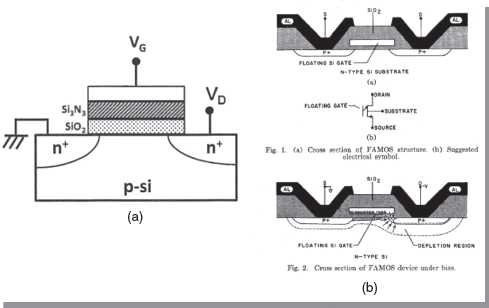
Figure 3(a) MNOS structure (Wegener et al.): discrete charge trapping devices (Courtesy of Simon Sze) and Figure 3(b) Floating gate Avalanche-injection MOS (FAMOS) structure [6]
From the 1960’s to the beginning of the 1970s, only mask writable memories (Read Only Memories or ROMs) were available. Electrically programmable/erasable devices were still confined in their infancy. In 1971, Intel proposed a 2kBit Floating gate Avalanche-injection MOS (FAMOS) memory [6], without a control gate, to store charge from the MOSFET drain (Figure 3b) by using a carrier injection from the avalanche current at the drain. Pulses of 50 V for 5 ms, with a load current of 50 mA, were necessary to program 1 bit. The memory was UV erasable collectively but still needed to be programmed bit by bit, due to its NOR gate architecture. However, the absence of a control gate could not make it electrically erasable.
2. The advent of Flash memories
Fujio Masuoka was an intellectually precocious child, especially good at math, had overwhelming capacities by three years in advance at the school and high school levels. He was thus a very curious spirit and certainly keen to taking risky paths for innovation. Early in his career at Toshiba, he worked on DRAM as a development engineer as well as a salesman.
At that time, Ultraviolet (UV)-EPROM and EEPROM were available. However, there were cost per bit issues with UV-EPROM and EEPROM. EEPROM needed a much more complex architecture (two transistors) than UV-EPROM, which were more compact and scalable. However, UV-EPROMs posed more constraint at the system level (UV collective erasing) and made them less popular.
“My idea on EPROM was that programming can be performed at a lower voltage and a higher speed than that of the conventional EPROM, by using a control gate. In the invention USP 3,825,945 I claimed that the capacitance between the floating gate and control gate should be larger than that between the substrate and floating gate [7]” says Masuoka. An increased coupling ratio (ratio between the control gate/floating gate capacitance and floating gate/substrate capacitance) resulted in enhanced charge injection into the floating gate from the device channel. Moreover, Masuoka and Iizuka proposed to use stacked polysilicon electrodes separated by a coupling insulator to implement the control and a floating storage gate [8–10], in a one transistor cell programmable in a drain avalanche mode. The Stacked-gate Avalanche-injection MOS (SAMOS) memory established a direct link with polysilicon gate CMOS, which was becoming the mainstream technology (Figure 4a). These conditions, put together, formed the concept for a future commodity-like product that was never thought, but finally proven to be capable of competing with DRAM in terms of density and cost per bit, even though not as fast. The success of the digital cameras, of the flexibly mobile mass storage in the form of USB keys, and of mobile phones, boosted the demand for such devices easily usable by the public at large. This demand was enabled by Flash Memories. However, at this point, still the “battle was not won”!
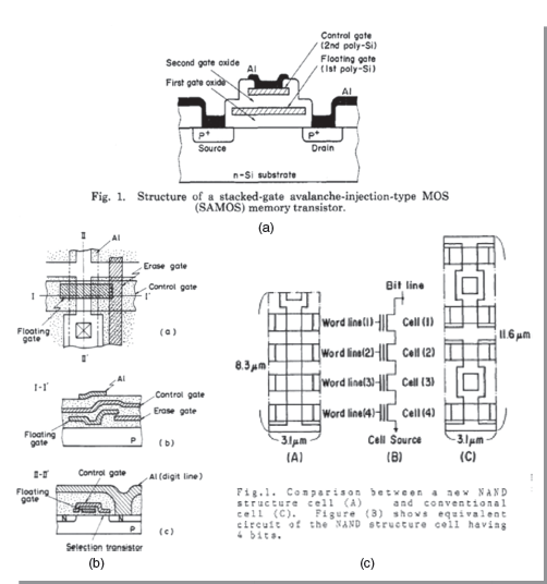
Figure 4 (a) SAMOS structure [9] programmable by charge injection resulting from drain avalanche breakdown and electrically or UV erasable—partially presented at IEDM 1972 late news; (b) First paper on Triple poly Flash Memory (NOR gate), presented at IEDM 1984 [12]; (c) First paper on NAND type Flash Memory, presented at IEDM 1987 [15]. Comparison between NOR and NAND gates layout. will be details of Fig.4b visible after printing?
In the early 1980s, the EEPROM required two transistors per bit (a non-volatile memory transistor and a select transistor) necessarily bit by bit rewritable. How could each bit be reduced to one non-volatile memory transistor only to reduce the bit cost? “The cost per bit could drop much lower to a quarter,” declares Masuoka who paradoxically underlines: “I noticed that by erasing all bits at once, and then writing bits on a per-bit basis, a select transistor would not be needed. This marked the advent of electrically-rewritable Flash Memory, which can be erased all at once, with only one non-volatile memory transistor for each bit, granted as USP 4,437,174 [11].” This conclusion was counter-intuitive even for many professionals because erasing all bits in a sector to change one was seen as a “waste of time”. The erasure was obtained by injecting electrons by field emission between the control gate and a third polysilicon erase gate. Actually, at the small scale of writing/erasing times, collective Flash erasure was not an issue and was energy wise efficient. The working principles behind NOR flash memory were presented at the 1984 IEDM [12] (Figure 4b), and 256-kbit NOR flash memory was announced at the 1985 ISSCC [13].
Masuoka adds: ”In 1986, I eventually noticed that NOR flash memory was so insufficiently low cost that it could not drive out magnetic disks, and that the Flash Memory should be needed to further reduce the cell area per-bit. The answer was NAND Flash Memory, granted as USP 5,245,566 [14]. In April 1987, I successfully verified the basic properties of the NAND flash memory, namely writing, reading and erasure by bulk injection.” The results were presented at the 1987 IEDM [15] (Figure 4c)
Masuoka wanted to quickly prototype a 4Mbit NAND Flash circuit, but had a hard time to convince his management to provide mask funding. He failed to get any funding from the computer division, because they found the concept too ambitious to replace magnetic storage memories.
“If I’d given up there, all my work up to then would have come to nothing,” confesses Masuoka. He found an ally at the Consumer Electronics Division to financially support his project: “I explained to Mr. Tajiri, Director of the Consumer Electronics Laboratory, that if we managed to produce 4-Mbit NAND flash memory, cameras would no longer need film. I was indeed explaining that the digital cameras which we know today would become possible. We successfully developed 4-Mbit NAND flash memory in 1988 and announced 4-Mbit NAND flash memory at the ISSCC in February 1989 [16]. Thereafter, Mr. Tajiri used the 4-Mbit NAND Flash memory to launch the world’s first digital camera to replace conventional film with NAND flash memory. At the time, the price of the flash memory was high and the world’s first flash memory-based camera didn’t sell well.”
Masuoka finally concludes: “Now, Flash Memory is penetrating into the whole economic framework. The world-wide market size of the NAND Flash Memory last year surpassed $52B. In the near future it is expected to become more than $100B, which is unmatched in the history of the world, when all the HDD’s in the personal computers are replaced by the SSDs, and the HDD’s of the data station of Google and FaceBook, etc. are partially replaced by the SSDs. This is because the market share of not only the semiconductor memory but also the HDDs is accounted. And also, many power stations in the world can be saved by replacing the HDD by the SSD. For this is what the final target of the NAND Flash Memory is all about, and there is no doubt at all that the NAND Flash Memory is an earth-conscious ‘Green Technology’.”
3. Looking for new breakthroughs in process integration
At the beginning of the years 2000, the quest for an efficient solution to increase the capacity of floating gate based Flash Memories beyond the 70–50 nm node has been an ongoing question. As a matter of fact, the high voltage used for cell programming/erasing and the floating gate architecture itself, imposed insulators thicker than for logic devices to withstand the reliability constraints. Such a situation made the floating gate transistors more sensitive to short channel effects and to a retention and endurance degradation due to Stress Induced Leakage Current (SILC). Cell to cell disturbance increased with spacing reduction. At such a point, several alternatives were making sense to move aside the necessity of 2D linear scaling to increase memory capacity. Beyond stacking 2D memory arrays in a package, other device architecture or integration based solutions were being developed. One idea was to increase the number of bits per cell [17] by programming several states corresponding to several threshold voltages to read, the limit being the threshold voltage distribution variability and the associated noise margins. Nowadays, up to 4 bits per cell are implemented in large capacity SSD circuits (see hereunder). Another way was to stack 2D arrays at the chip level [18], with a limit in a cost per bit reduction approach.
Finally, a multiplication of vertical 3D strings Flash architecture was proposed by Toshiba [19] by the so called Bit Cost Scalable (BiCS) technology, renamed BiCS FLASHTM. The vertical gate-all-around transistor architecture with discrete traps (pseudo floating gates) storage had a higher electrostatic integrity than the conventional 2D architecture. Moreover, the vertical gate-all-around structure did not require such aggressive lithography capabilities to increase the final circuit capacity and resulted in a highly competitive cost per bit.
4. Three Dimensional (3D) Flash Memory: BiCS FLASHTM at TOSHIBA’s memory division1
At Toshiba, the BiCS FLASHTM technology was developed as soon as July 2005 when the first idea came out. Toshiba announced the first example of a vertical channel based high density Flash memory array, featuring gate all-around transistors and a SONOS like gate stack structure. As in all major memory companies, there were discussions on different options to solve the scaling issues of 2D Flash Memories: an increasing transistor variability, a program disturbance due to neighboring cell interferences, and an increasing fabrication tools cost. Options such as 3D stacked floating gates, FeRAM, ReRAM, PCRAM were being considered in the discussion. In that context, a cross-point architecture was published by Matrix Semiconductor (now Sandisk), composed of cross-bar type one-time programmable memory cells, stacked repeatedly [20]. At that time, Hideaki Aochi was leading a non volatile memory process integration team at Toshiba. Note that the company has recently spun off its memory business by creating KIOXIA.
Aochi, now a KIOXIA engineer, recalls: “The cross point architecture needed a large number of process steps, because of the large number of repetitions of the similar cross-bar shaped memory structure. A large fabrication chip cost was a severe issue.”
Aochi remembers: “One day, during my ride in the commuter train, I had gotten the basic idea of punch and plug process to make a hole thru many stacked layers of two different materials. Then our team had started to construct all the elements of the basic concept of BiCS FLASH6, which are: detailed process integration, device design, array structure, staircase layout, and row/column wiring connection to driver and sensing circuit.” (Figures 5, 6).
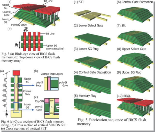
Figure 5 First publication of the BiCS FLASHTM Memory technology at VLSI Technology Symposium in June 2007 [19].
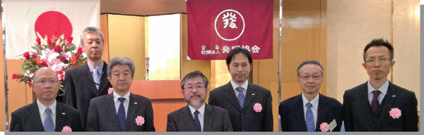
Figure 6 Members of the BiCS FLASHTM Memory team celebrated at KIOXIA. From left to right: (Lower row) Masaru Kito*, Tomoharu Matsushita**, Hideaki Aochi*, Hiroyasu Tanaka*, Akihiro Nitayama*, Ryota Katsumata* and (Upper row) Masaru Kido*; *Inventor, ** Chief Production Executive of KIOXIA Corporation (by permission of KIOXIA)
Many questions arose while starting to implement such a seductive idea: the impact of a polysilicon channel on variability and the process integration of a vertical gate-all-around transistor. Since the 1980s, at the time of advent of thin film p-channel transistors load for Static RAMs or displays row- and column-select transistors, the use of polysilicon channels in the fabrication of logic or memory circuits of ULSI densities was highly challenging and many questions existed around on a possible variability issue. These types of devices were better known in the field of displays but for much larger geometries.
Aochi says: “After some experiments, we realized that the variability of transistor performance had been caused by two major factors, one was due to the poly-Si channel, as we had expected, and the other was the contact resistance of the connection of the poly-Si channel to the substrate.”
The solution was to give a hollow tubular shape to the memory strings and to thin down the polysilicon channel to keep electrostatic integrity, just as in a thin body SOI transistor. Typical macaroni shaped channels were thus implemented. A pipe-shaped string structure could eliminate the bottom contact of the poly-channel to the substrate and stabilize the variability of the contact resistance.
The first results of an experimental 512 kbit test chip were presented at the 2007 VLSI Symposium [19]. The team was successful in presenting the results of functional 32 Gbit density memory arrays, obtained in 2008, at the 2009 VLSI Technology Symposium [21].
Aochi underlines: “That announcement impacted all of flash memory manufacturing and accelerated similar type of flash memory development. We had made the first production chip of 48-layers of BiCS FLASH6 with 256 Gbit memory density in 2015.” Obtaining reproducible hole shape strings was a major critical path.
Toshiba announced at ISSCC 2019 a 1.33 Tbit chip based on the 3D BiCS FLASHTM technology stacking 96 layers and 4 bit/cell [22].
After the successful implementation of the BiCS-FLASHTM technology by Toshiba and continued by Kioxia, 3D vertical Flash memories have become very popular for mass storage among the main memory makers. After producing stacked 2D structures [18], Samsung followed an approach close to Toshiba’s and demonstrated a vertical 3D structure integrating a damascene p+-like W gate, ancestor of a vertical TaNOS structure [23].
Nowadays, 3D Terabit class memory can be integrated in a single chip, stacking up to 128 layers, featuring up to 4 bits/cell and a bit surface density approaching 10 Gbit/mm2. The memory circuits can be handheld in a solid state disk or equip mass storage systems in data centers. The 3D string-type Flash Memories have been adopted among Toshiba/KIOXIA competitors as well, either with a SONOS/p+-like TaNOS or vertical Floating gate structures [23]–[26].
Many other candidates featuring alternative structures or materials have been trying to take over their success. These are floating gate-inspired (i.e. Si Nanocrystal FG, split gate, NROM structures, etc.) or based on 1 to 2 transistors associated to a resistor or capacitor(s) (i.e. MRAMs, STT RAMs, ReRAMs, FeRAMs, etc.) to reduce the SILC issue or address a storage node. Their compatibility or co-integration with Si CMOS is sometimes a strong requirement. Some of these alternative solutions could be or have already been adopted as application specific, field programmable gate arrays (FPGAs), embedded memories or distributed in CMOS for new computing paradigms and ultra low power circuit architectures (i.e. neuromorphic computing and programmable circuits, non-volatile logic and RAMs, etc.) [27]. These latter topics have not been addressed in this issue, due to the vast extent of the subject, as they would request another article.
The discovery of the Floating Gate and discrete trapping concepts augmented by the invention of Flash Memories are with no doubt major events in the history of microelectronics and its success. They have sustainably impacted our daily life with broad societal usage. Their most recent success for 3D mass storage was possible thanks to a succession of microelectronics engineering marvels developments.
Acknowledgements to Prof. Simon Sze (NCTU), Prof. Fujio Masuoka (Tohoku University), Dr. Koji Sakui (Honda), Prof. Masaaki Inutake (Tohoku University), Drs. Hiroyasu Tanaka, Ryota Katsumata, Hideaki Aochi, and Kazunari Ishimaru (KIOXIA).
References
[1] S.M.Sze, “Physics of Semiconductor Devices”, Ed. John Wiley and Sons Inc., New York (1969).
[2] D. Khang and S.M. Sze, “A floating gate and its application to memory devices,” Bell Syst. Tech. J. Briefs, pp.1288–1295, vol. 46, Aug. 1967.
[3] H. A. R. Wegener, A. J. Lincoln, H. C. Pao, M. R. O’Connell, R. E. Oleksiak, H.Lawrence, “THE VARIABLE THRESHOLD TRANSISTOR, A NEW ELECTRICALLY-ALTERABLE, NON-DESTRUCTIVE READ-ONLY STORAGE DEVICE,” Digest. Tech. papers IEDM 1967, #11.4, p.70.
[4] J.R. Szedon and T.L. Chu “Tunnel Inspection and Trapping of Electrons in Aluminum-Silicon Nitride- Silicon Dioxide-Silicon (MNOS) Capacitors,” Abs. Solid State Device Research Conference, p 631, 1967.
[5] B.V. Keshavan and H. C. Lin, ”MONOS MEMORY ELEMENT,” IEDM Digest of Technical Papers, pp. 140–141, Oct 1968.
[6] D. Frohman-Bentchkowsky “A fully-decoded 2048-bit electrically-programmable MOS ROM,” IEEE ISSCC Digest of Technical Papers, pp. 80-81, Feb. 1971 and IEEE JSSC pp 301–306, Oct 1971.
[7] F. Masuoka, “Field Effect Semiconductor Memory Apparatus with a Floating Gate,” USP 3,825,945, July 23, 1974.
[8] H. Iizuka, T. Sato, F. Masuoka, K. Ohuchi, H. Hara and Y. Takeishi, “A Fully-Decoded 2048-Bit Avalanche-Injection Type, Electrically Alterable ROM,” IEDM Tech Digest pp. 4–5, 1972.
[9] H. Iizuka, T. Sato, F. Masuoka, K. Ohuchi, H. Hara and Y. Takeishi, “A Fully-Decoded 2048-Bit Avalanche-Injection Type, Electrically Alterable ROM,” IEEE TRANSACTIONS ON ELECTRON DEVICES, VOL. ED-23, NO. 4, pp.379–387
[10] F. Masuoka and H. Iizuka, “Semiconductor Memory Device,” USP 4,115,795, Sep. 19, 1978.
[11] F. Masuoka, “Semiconductor Memory Device,” USP 4,437,174, Mar. 13, 1984.
[12] F. Masuoka, M. Asano, H. Iwahashi, T. Komuro and S. Tanaka,“A new Flash EEPROM cell using triple polysilicon technology,” IEEE Tech. Dig. IEDM 1984, pp. 464–467.
[13] F. Masuoka, M. Asano, H. Iwahashi, T. Komuro and S. Tanaka, “A 256K Flash EEPROM using triple polysilicon technology,” IEEE ISSCC 1985, pp. 168–169.
[14] F. Masuoka, “Programmable Semiconductor,” USP 5,245,566, Sep. 14, 1993. This patent showed NAND Flash Memory.
[15] F. Masuoka, M. Momodomi, Y. Iwata, and R. Shirota, “New ultra high density EPROM and Flash EEPROM cell with NAND structure cell,” in IEEE Tech. Dig. IEDM 1987, pp. 552–555.
[16] Y. Itoh, M. Momodomi, R. Shirota, Y. lwata, R. Nakayama, R. Kirisawa, T. Tanaka, K. Toita, S. Inoue, and F. Masuoka, “An experimental 4Mb CMOS EEPROM with a NAND structured cell,” IEEE Int. Solid-State Circuits Conf., 1989, pp. 134–135.
[17] M. Bauer, R. Alexis, G.Atwood, et al., “A Multilevel-Cell32Mb Flash Memory,” Tech Digest IEEE Int. Solid-State Circuits Conf, 1995 , p132–133.
[18] SM Jung, J Jang, W Cho et al., “Three dimensionally stacked NAND flash memory technology using stacking single crystal Si layers on ILD and TANOS structure for beyond 30nm node,” Tech Digest IEDM, 2006 , p37–40.
[19] H.Tanaka, M.Kido, K.Yahashi et al., “Bit Cost Scalable Technology with Punch and Plug Process for Ultra High Density Flash Memory,” Symp. on VLSI Tech. Dig., pp14–15, 2007.
[20] Mark Johnson, Ali Al-Shamma, Derek Bosch et al., “512-Mb PROM With a Three-Dimensional Array of Diode/Antifuse Memory Cells,” IEEE JOURNAL OF SOLID-STATE CIRCUITS, VOL. 38, NO. 11, pp.1920–1928, NOVEMBER 2003.
[21] Ryota Katsumata, Masaru Kito, Yoshiaki Fukuzumi et al., “Pipe-shaped BiCS Flash Memory with 16 Stacked Layers and Multi-Level-Cell Operation for Ultra High Density Storage Devices,” Symp. on VLSI Tech. Dig, pp 136–137, 2009.
[22] N. Shibata , K. Kanda, T. Shimizu et al., “A 1.33Tb 4-bit/Cell 3D-Flash Memory on a 96-Word-Line- Layer Technology,“ ISSCC 2019 Tech Digest,pp 210-212.
[23] Jaehoon Jang, Han-Soo Kim, Wonseok Cho, et al., “Vertical Cell Array using TCAT (Terabit Cell Array Transistor) Technology for Ultra High Density NAND Flash Memory,” Symp on VLSI Technology Symp. Digest of Technical papers, (2009), pp 192–193.
[24] D-H. Kim, H. Kim, S. Yun, Y. Song et al., “A 1Tb 4b/Cell NAND Flash Memory with tPROG = 2ms, tR = 110μs and 1.2Gb/s High-Speed IO Rate,” To be published at IEEE ISSCC 2020.
[25] H. Huh, W. Cho, J. Lee, Y. Noh et al. “A 1Tb 4b/Cell 96-Stacked-WL 3D NAND Flash Memory with 30MB/s Program Throughput Using Peripheral Circuit Under Memory Cell Array Technique,” To be published at IEEE ISSCC 2020.
[26] K. Parat and A. Goda, “Scaling Trends in NAND Flash,” IEDM Tech. Dig., pp. 2.1.1-2.1.4, 2018.
[27] S. Deleonibus, O. Faynot, T. Ernst et al.,“Future Challenges and Opportunities for Heterogeneous Process Technology. Towards the Thin Films, Zero Intrinsic Variability Devices, Zero Power Era,” IEDM Tech. Dig., pp. 9.2.1-9.2.4, 2014.
1 Currently spun off from Toshiba and renamed as KIOXIA.