Technical Briefs
Marvels in MEMS Evolvement
and Development—Silicon as a
Micromechanical Material has
been Driving More-than-Moore
by Joachim N. Burghartz
In the past issues of the EDS Newsletter, since July 2018, we were pointing to marvels in microelectronic engineering that were associated with original contributions coming as a surprise, or having an unexpectedly high impact. All of them were related to driving Moore’s Law, making silicon devices smaller and squeezing more electronics on a silicon chip, and all of them were primarily technical. But how about MEMS? Microelectromechanical devices had little to do with mainstream microelectronics in the 1950s through 1970s. At Bell Labs, Uhlir looked into etching of bulk silicon and made the first steps into bulk micromachining [1]. Robbins and Schwartz from Hughes Semiconductors published in 1960 on chemical etching of silicon [2]. Richard Feynman’s famous talk ‘There’s plenty of room at the bottom’ [3] may have inspired the development of the first MEMS devices, such as Wilfiger’s Resonistor [4] and Nathanson’s Resonant Gate Transistor [5]. Nathanson’s work can be considered the first step into surface micromachining, in which the planar wafer processes were exploited for shallow three-dimensional micromechanical structures on top of the bulk silicon wafer. Further advancements in bulk micromachining by Waggener [6] and others, led in the 1970’s to the development of pressure sensors [7], inkjet nozzles [8] and other MEMS devices.
However, these achievements came from isolated efforts; there was no MEMS technical community and no focused industrial effort that could be compared to the well coordinated miniaturization of microelectronics following Moore’s Law. And the term MEMS was not even created. This clearly changed with Kurt Petersen’s article ‘Silicon as a Mechanical Material’ [9] which appeared in the Proceedings of the IEEE in 1982. It was the time when Moore’s Law was endangered as Hg-based lithography steppers seemed not extendable beyond i-line. There was a clear desire for leveraging silicon technology through new businesses, the first steps into More-than-Moore. Petersen’s Proceedings paper can be considered a true marvel in microelectronic engineering since it led to pulling together isolated efforts into a research community, by driving industrial applications, by encouraging start-ups and by putting MEMS on the semiconductor roadmap. In recognition of these efforts and successes, Kurt Petersen was honored by receiving the 2019 IEEE Medal of Honor, the highest-level award issued by the IEEE. Petersen’s career on MEMS is well described in a recent article in IEEE Spectrum [11]:
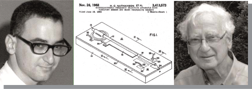
Harvey Nathanson at young age (left) and more recently (right), next to his early MEMS device (middle) [9]
Kurt Petersen, after graduating from MIT, had joined IBM’s Almaden Research Center in 1975 to work in an optics group, but he found himself bored. With an open eye for new opportunities he once came across a huge black stain on the floor which he tracked down as an ink spill caused by another group working on inkjet nozzles. He launched himself down a new career path, building MEMS technologies. Kurt read papers on silicon micromachining and got in touch with the researchers. He remembers: “Ernest Bassous at IBM, Ken Bean at TI, Larry Hornbeck at TI, Harvey Nathanson at Westinghouse, Prof. Jim Angel at Stanford, Prof. Ken Wise at Michigan, Prof. Richard Muller at Berkeley, Prof. Wen Ko, Prof. Steve Senturia at MIT, Prof. Masayoshi Esashi at Tohoku University—these were some of my early heros in the MEMS arena.” He identified lots of micromechanical structures and devices that were likely useful to IBM, but his employer was not interested. On the contrary, many people doing crazy things on silicon were finding him. Petersen turned into a technology evangelist for MEMS. At the time the proceedings paper was published, only 30 to 40 researchers around the world were working in that field. By 1990, that number had ramped up to about 600. Kurt Petersen himself contributed to growth of the field by founding six start-up companies; Transensory Devices was his first, SiTime was his most successful one. He told me: “The best story is SiTime. SiTime builds MEMS oscillators which are gradually replacing the quartz crystal. These devices are now better than the quartz crystal oscillator in every way, frequency stability, temperature performance, size, cost, reliability. SiTime has shipped cumulatively over 1B units.” Kurt Petersen himself, as somebody driving an entire field, can be considered a personified marvel of microelectronic engineering, or better, of silicon technology. When confronting Franz Laermer, the co-inventor of the BOSCH RIE process to be addressed later in this article, he said: “A careful definition of “successful” is required in this place: Is it about money? About technical impact? When it comes to money, SiTime is certainly not the most successful one of Kurt Petersen. Maybe the fanciest one, most innovative, with the largest impact. Kurt also co-founded NovaSensor (together with Janusz Bryzek and Joseph Mellon). This company was later bought by LUCAS for a tremendous amount of money, as far as I know at a higher price than that of SiTime later on. The most successful start-up company from the monetary value which Kurt ever founded was Cepheid. Cepheid was traded at ~$4B at the NASDAQ stock-exchange under the ticker-symbol CPHD, and was finally taken over by another company in a similar price-regime around $5-6B.”
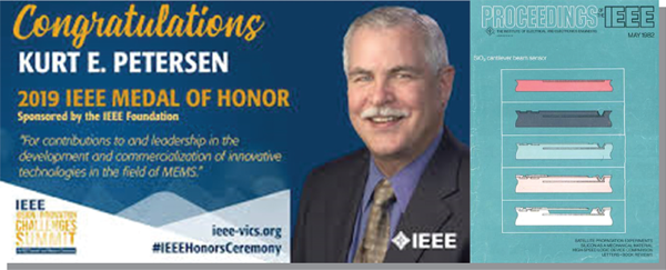
Kurt Petersen (left), recipient of the 2019 IEEE Medal of Honor, and the cover of Petersen’s 1982 paper in the Proceedings of the IEEE [10], [11]
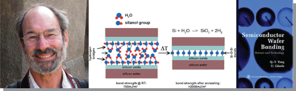
Jerry Lasky (left; courtesy of J. Lasky rep Radaris), scheme of silicon fusion bonding (SFB) (middle, [14]), and cover of Ulrich Gösele’s book on SFB [15]
When looking at what he had been influencing, Kurt Petersen said: “Silicon Fusion Bonding (SFB) and Deep Reactive Ion Etching (DRIE) have had the most impact on modern MEMS. SFB was invented at IBM [12] and Toshiba [13] around 1982 for SOI circuits. At NovaSensor, we used this technology to build MEMS devices for the first time. In fact, we invented the term Silicon Fusion Bonding. I still remember a group of us sitting around brain-storming names for this new process. At the time, Toshiba was calling it Direct Wafer Bonding. But, SFB became the preferred terminology. DRIE was invented by Franz Laermer at Bosch in about 1992.”
When thinking about silicon wafer bonding, we may all be thinking of a coincidental discovery. It may have happenend to many of us that by accident two polished silicon wafers ended up in the same slot of a wafer carrier. Without any doubt, those two wafers would easily bond together and could not be separated afterwards. However, Jerry Lasky, now happily retired and kayaking and hiking in Vermont but formerly with IBM and the key inventor of SFB, told me: ”The discovery of wafer bonding was not as accidental as you are imagining. I think it is a case of “chance favors the prepared mind.” I was trying to do wafer bonding, being familiar with “Mallory Bonding” of wafers to glass where a voltage is placed across the system; it is heated to 350 °C and bonding occurs. However, that relies on Na+ in the glass to be a conductor. I was guessing that at high enough temperatures Na+ would not be needed. I was trying to bond an oxidized wafer to a second wafer in a test run in a furnace at 1000 °C. The wafers were in contact, but the electrodes not energized. Despite this, the wafers came out bonded! I repeated several times with the same result. This was a “research” furnace which is certainly not the cleanest system. I assumed a contaminate was playing a role. I finally got access to clean equipment and was able to show that, if I had a glass rod between two wafers but removed it prior to insertion to the furnace, they came out bonded. However, if I inserted them into the furnace held apart and removed the glass rod after they were heated to 600 °C or above, they did not bond. This was consistent with OH ions absorbed on the surface contributing to the bonding. The bonding part of the process was quite well developed and very repeatable by 1984. This is described in our 1985 IEDM paper [12].”
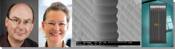
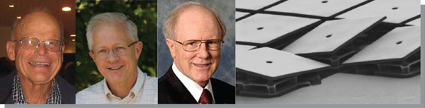
Franz L¤rmer and Andrea Urban (Schilp) (left; IEEE Jun-ichi Nishizawa Medal Recipients web site), a typical etch profile resulting from the BOSCH DRIE process (middle; open content Wikimedia Commons), and a deep trench used for a high-density DRAM formerly manufactured by Infineon AG (right; courtesy Infineon AG)
Richard Muller and Roger Howe (two left) pioneered polysilicon surface micromachining.
Larry Hornbeck (photo on the right) pioneered micro mirrors and TI’s digital light processing device (right)
Deep Reactive Ion Etching was invented and developed by Bosch engineers Franz Laermer and Andrea Urban (Schilp) [16] primarily for application to MEMS but also had a tremendous impact on DRAM technology in allowing for very high aspect ratio trench capacitor formation and on Through-Silicon-Vias (TSV) for three-dimensional (3D) circuit integration. Franz Laermer remembers: ”The development was a R&D project at Bosch Corporate Research. Andrea Urban’s and my work was strongly supported and encouraged by our department head, Dr. Gerhard Benz at that time. He once said to me: ‘Your task is like struggling for the quadrature of the circle – nearly impossible to succeed. But if you make it a success, the impact would compensate for any efforts’. In fact, the efforts were minor, financially speaking: 2 people over some years, and a very limited materials budget, because we built our own provisory constructions at low cost and did not request expensive purchases.” Different from Waggener’s anisotropic wet etching following the crystalline structure of silicon, the DRIE or BOSCH process allowed for vertical etch profiles in any orientation, independent from the crystalline structure. The plasma process is based on consecutive short steps of polymer deposition for sidewall protection, and etch steps with energetic ion impact to remove the polymer from the planar regions.
In addition to Petersen’s mentioning of SFB and DRIE as marvels in MEMS, I would like to bring up polysilicon surface micromachining introduced by Howe and Muller in 1983 [17]. Polysilicon and silicon dioxide are generally used as active and sacrifical layers to build up complex micromechanical structures on top of the wafer surface. This technological concept had an unexpected impact on the emergence of MEMS. Three-dimensional microstructures became feasible through first building them up and finally releasing them by removing the sacrificial material. Prominent examples are the Digital Light Processing (DLP) device invented by Larry Hornbeck at Texas Instruments [18], [19], the Analog Devices and Bosch inertial sensor product lines, electrostatically actuated micro gear devices [20], micromechanical resonators [21], and implantable medical neuro probes [22].
In conclusion, MEMS as a whole can be considered a marvel of microelectronic engineering, or more generally of silicon technology, because it features the foundation of what we call now ‘More-than-Moore.’ For this it took the early efforts and indications of what else could be done with silicon technology beyond integrating electronic functions at ever increasing density and performance, such as Nathanson’s first MEMS device in the 1960’s. It needed Petersen’s vision and entrepreneurship to give birth to the MEMS community in the 1970’s, and it took the numerous efforts thereafter from the 1980’s to indentify and develop MEMS technologies and applications that led to an unexpectedly high economic value. There is more to come.
References
[1] A. Uhlir, “Electrolytic Shaping of Germanium and Silicon,” Bell Labs Technical Journal, (1956), vol. 35, no. 2, pp. 333–347.
[2] H. Robbins and B. Schwartz, “Chemical Etching of Silicon,” Journal of Electrochem. Soc., (1960), vol. 107, no. 2, pp. 108–111.
[3] R. Feynman, “There is plenty of room at the bottom,” Lecture at the American Physical Society meeting at Caltech on December 29, 1959.
[4] R.J. Wilfinger, P. H. Bardell, D.S. Chhabra, “The Resonistor: A Frequency Selective Device Utilizing the Mechanical Resonance of a Silicon Substrate.” IBM J. Res. Dev. Vol. 12, no. 1, (1968), pp. 113–118.
[5] H.C. Nathanson, W.E. Newell, R.A. Wickstrom, J.R. Davis, “The Resonant Gate Transistor,” IEEE Trans. El. Dev., (1967), vol. 14, no. 3, pp. 117–133.
[6] H.A. Waggener, R.C. Krageness, A.I. Taylor, “Anisotropic Etching of Silicon for Forming Isolation Slots in Silicon Beam Leaded Integrated Circuits,” in Techn. Dig. Of IEEE Int. El. Dev. Mtg., (1967), pp. 68.
[7] A.C.M. Gieles and G.H.J. Somers, “Miniature pressure transducers with a silicon diaphragm,” Philips Tech. Rev., (1973), vo. 33, pp. 14–20.
[8] E. Bassous, H. H. Taub, and L. Kuhn, “Ink jet printing nozzle arrays etched in silicon,” Applied Physics Letters, (1977), vol. 31, no. 2, pp. 135–137.
[9] The Future Markets Magazine “Learning from pioneers: The father of the MEMs - In conversation with Harvey C. Nathanson;” The Quintessence of Wearable Technology Magazine, (2016) Issue 18, pp. 87-88.
[10] K. Petersen, Kurt, “Silicon as a mechanical material,” Proceedings of the IEEE, vol. 70 no. 5, (1982), pp. 420–457.
[11] Tekla S. Perry, “The Marvelous MR. MEMS—An ink stain led Kurt Petersen, 2019 IEEE Medal of Honor recipient, to a lifetime of building microdevices,” IEEE Spectrum, (2019), vol. 56, no. 5, pp. 44–51.
[12] J.B. Lasky, S.R. Stiffler, F.R. White, J.R. Abernathy, “Silicon on insulator (SOI) by bonding and etchback,” in Tech. Dig. Internat. El. Dev. Mtg., (1985), pp. 684–687.
[13] M. Shimbo, K. Furukawa, K. Fukuda, K. Tanzawa, “Silicon-to-silicon direct bonding method,” Journal of Applied Physics, (1986), vol. 60, no. 10, pp. 2987–2989.
[14] S.H. Christiansen, R. Singh, U. Gosele, “Wafer Direct Bonding: From Advanced Substrate Engineering to Future Applications in Micro/Nanoelectronics,” Proceedings of the IEEE, (2006), vol. 94, no. 12, pp. 2160–2106.
[15] Q.-Y. Tong and U. GÖsele, “Semiconductor Wafer Bonding,” Wiley-Interscience, (1998), 320 pages.
[16] F. Laermer and A. Schilp, “Verfahren zum anisotropen ¤tzen von Silicium,” German Patent DE 42 41 045.
[17] R. T. Howe and R. S. Muller, “Polycrystalline Silicon Micromechanical Beams.” Journal of the Electrochemical Society, (1983), vol. 130, no. 6, pp. 1420.
[18] L.J. Hornbeck, “128 X I28 Deformable Mirror Device,” Transactions on Electron Devices, (1983), vol. 30, no. 5, pp. 539–545.
[19] L.J. Hornbeck, “Deformable-Mirror Spatial Light Modulators (Invited Paper),” Spatial Light Modulators and Applications III, SPIE Critical Reviews, (1989), vol. 1150, pp. 86–102.
[20] L.-S. Fan, Y.-C. Tai, R.S. Muller, “IC-Processed Electrostatic Micromotors,” Techn. Dig. Internat. El. Dev. Mtg., (1988), pp. 666–669.
[21] W.C. Tang, T.-C.H. Nguyen, R.T. Howe, “Laterally Driven Polysilicon Resonant Microstructures,” Sensors and Actuators, (1989), vol. 20, pp. 25–32.
[22] K. Najafi and K.D. Wise, “An implantable multielectrode array with on-chip signal processing,” IEEE Journal Sol. St. Circ., (1986), vo. 21, no. 6, pp. 1035–1044.