Technical Briefs
System and High-Volume-
Manufacturing Driven More
Moore Scaling Roadmap
1. Introduction
Scaling device features by approximately 30% in each new technology generation supported Moore's Law doubling the number of transistors every 2-years for decades while also improving system performance by concurrently increasing transistor drive current and reducing operating voltage. This combination allowed introduction of new functions in innovative System-On-Chip (SoC) products with better performance and lower cost. The progress of technology scaling has been measured by monitoring PPAC (Performance-Power-Area-Cost) improvements, typically happening with any new technology introduction with a cadence of 2‐3 years. However, pure geometric scaling does not provide any longer the necessary PPAC improvements at the system level due to several reasons:
The ITRS established in 1998 was mainly aimed at transistor density and performance improvements by means of scaling but in this decade the roadmap projections have been re-focused on system constraints; this consideration led to the restructured International Roadmap for Devices andSystems (IRDS). This collection of documents provides the roadmap for logic devices, on-chip interconnect, and memory devices driven by feasible manufacturability routes and system integration requirements.
2. Market Drivers of More Moore Scaling and Roadmap Process
System considerations and cost optimization requirements have driven the need for a unified technology platform where high-performance digital logic needs to enable server applications are considered and also provide support for low power needs to enable mobile computing for the edge applications. Both requirements must be kept into account with equivalent relevance to allow the electronics industry to continue growing at historical (or better) rates. Therefore the mission of the IRDS More Moore (MM) IFT chapter is to provide physical, electrical, and reliability requirements for a unified logic and memory technology platform to sustain power, performance, area, cost (PPAC) “scaling guidelines” for mobile and cloud applications over a time horizon of 15 years for Mainstream/High-Volume Manufacturing (HVM) [1]. Such technology platform identifies the main technology drivers and provides the enabling tools for the following application (Fig. 1):

Fig. 1. Two pillars of More Moore application drivers.
More Moore (MM) roadmap guidelines identify technology enablement items for improving the system performance, power, and area in a timely manner; meeting a mobile product cadence of one year, maybe even six months, while providing a scalable product platform for the servers, which must be surviving 10 years, for multiple cloud applications. The first step in the roadmap process is to identify the ground rules and their inherent limits set by the unit process modules, devices, and the impact of any parasitics on performance. The second step is to describe the standard cell scaling parameters and how to further tighten key design rules by means of Design Technology Co-Optimization (DTCO). The third step is then the identification of device architecture and interconnects technology drivers to satisfy System-On-Chip requirements. Finally, optimization of all the above elements brings performance and careful energy management together to collectively enable cost effective system scaling. Since transistor technology alone is no longer sufficient to satisfy the requirements for enhanced memory bandwidth, IO, and outside connectivity demanded by system driven requirements, it is necessary to introduce new 2.5D/3D integration schemes. These integration technologies enable the effective adoption of the needed memory with sufficient bandwidth, increased capacity, and latency parameters required for the various applications listed above. As the final step of this optimization process the various available enablement items are carefully analyzed and the essential items are down-selected to meet product delivery timeline while limiting process complexity to the most relevant innovative module processes to be added to the device technology platform in High-Volume-Manufacturing (HVM).
3. Ground Rules
Determination of ground rules is a critical step in defining both the unit process modules and a realistic economy of scaling [2]. It is of paramount importance to select a set of design ground rules that are as aggressive as possible and yet consistent with high yields in the High-Volume-Manufacturing (HVM) process to assure economic product viability. Lithography technology remains the key process step enabling reduction of device features. However, the limits of single exposure lithography were reached more than a decade ago and additional process steps had to be introduced to maintain scaling of device features by around 30% per technology generation. The most viable solution to achieve the required scaling goal through the years has resulted exposing multiple times any layers that exceeded the lithography capabilities. In few words for illustrative purposes let's consider exposing twice a set of lines and spaces; the first time the set of lines and spaces is exposed in the resist and then the same pattern is re-exposed a second time but offset by half pitch. The outcome is a set of interdigitized lines spaced at half the distance of the original ones. Under practical conditions more complicated sequences and mask combinations are required. This represents a viable engineering approach although it comes with the penalty of doubling or even quadrupling the lithography cost for any layer produced with this process method. Due to the rising process complexity associated with the multiple patterning it is important to carefully allocate the lithography technology to be used with each layer. The feature size that can be produced by any lithography tool is largely determined by the exposure wavelength. This means that design ground rules are determined by keeping into consideration the capability limits of the available lithography tool. For instance 76‐80 nm metal pitch can be obtained by using 193i immersion lithography tools (193 nm exposure wavelength) with double or even quadruple exposures. Similarly, 28‐30 nm metal pitch can be presently obtained by using EUV tools (13.5 nm) with a single exposure, but 18 nm pitch or lower may require double EUV exposure. These examples show the trade-off between exposure tool selection and design rules. Due to the much lower exposure wavelength of EUV it is possible to achieve much smaller ground rules for the EUV layers with much better tolerance margins as compared to double or quadruple exposure using tools exposing with 193nm wavelength. However, the selection of the lithography tool to be used by layer is not so obvious because careful cost considerations must be done since any exposure done by the EUV tool is as much as 3 times more expensive than the one of a 193i tool. Another careful consideration on how aggressively ground rules are to be scaled is due to considerations about the increased contributions of parasitics to the total performance. In summary, overlay and unnecessary scaling may bring diminishing returns on both transistor performance and also unnecessarily increasing power dissipation. This becomes the case even though area scaling may indeed reduce interconnects parasitics due to a reduction of wirelengths. All these trade-offs must be kept into careful consideration in the complex selection of ground rules (Fig. 2). 2D scaling is expected to eventually reach practical limits around the year 2030 when full 3D stacking technology is expected to become mainstream.
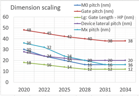
Fig. 2. Evolution of ground rules.
Correcting Nonsense Node Naming
The ITRS had defined technology nodes as the half-pitch of the smallest metal layer in any IC in the 90s. However, in the past 10 years several companies have redefined their own technology nodes by using much smaller numbers than the official definition. This method of naming nodes has by now lost any credibility since there is no longer any relation between the node name and any of the dimensions on the actual ICs that are being produced nowadays. For instance, several companies are talking about 7 nm technology node while in reality it should be named as 18 nm technology node corresponding to half of the 36 nm minimal metal pitch in the actual ICs.
It is important to note that there is no correlation between the naming convention (e.g. 7 nm, 5 nm technology) from different foundries and integrated device manufacturers (IDMs) and the technology capabilities in line with the PPAC requirements.
To further clarify this point the IRDS chose to name the by explicitly putting the key parameters used in defining the ground rules in the technology naming convention, these are: GxxMxxTx where Gxx represents the contacted gate pitch, Mxx represents the tightest metal pitch in nm and Tx represents the number of stacked tiers making up a 3D integrated transistor circuits. This notation illustrates the technology pitch scaling capability as well as 3D stacking capability [3]. On top of pitch scaling there are other elements of relevance such as cell height, Fin depopulation, DTCO constructs, 3D integration, etc. that define the target area scaling (gates/mm2), which will be explained in the next paragraph.
For sake of completeness the artificially defined industry technology nodes are indicated as a reference in the roadmap.
4. Standard Cell Architecture
As mentioned earlier design rules cannot be aggressively scaled down like in the past and therefore it is necessary to complement their role in reducing the area of the basic cell with novel layout techniques that allow to achieve the desired area reduction goal as well as producing more manufacturable design rules. This methodology is called Design Technology Co-Optimization (DTCO). The basic approach of DTCO consists in reducing the standard cell height and width by combining many design elements enabled by the technology. For instance, reducing the number of active devices in the cell and combining a limited scaling of the width of active devices as well as carefully applying a limited scaling of many secondary rules such as tip-to-tip, tip extension, PMOS-NMOS separation, and minimum metal area rules produce a drastic reduction of the cell height with substantial area savings. Recently further cell height reduction has been demonstrated by placing contact-over-active devices [4]. It is expected that in 2028 PMOS and NMOS devices could be stacked on top of each other allowing a further cell area reduction. This trend in standard cell height and width scaling is illustrated in Fig. 3 with the density scaling of standard cell shown in Fig. 4.
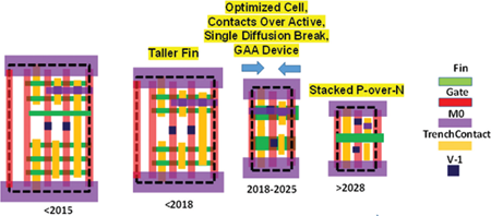
Fig. 3. DTCO-enhanced standard cell scaling evolution.
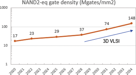
Fig. 4. Standard cell density scaling.
5. Device Structures
In the next 15 years it is forecasted that three phases of scaling will occur (Fig. 5): 1) Extending improvements of FinFET, 2) Transition to gate-all-around (GAA) devices, 3) Sequential integration (3DVLSI) of stacked devices. FinFET has continued to remain the key transistor architecture since 2011 and it will continue to remain the transistor architecture of choice until 2025 or so thanks to continuous electrostatics, drive current and cell architecture improvements such as increasing the Fin height and reducing the width of Fin to keep electrostatics under control [5][6].
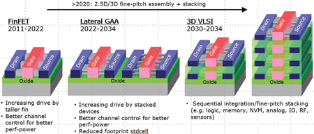
Fig. 5. Evolution of device structures.
In order to continue increasing performance and density it is necessary to increase the transistor output current and this requires improving the electrostatic control of the channel region while also reducing transistor footprint to increase layout density. To accomplish these tasks, it is necessary to make a transition from FinFET to Gate All Around (GAA) structures such as circular tubes or lateral nanosheets; the GAA transition is expected to gradually occur during the 2022‐2025 period. Such transition will require the introduction of new process modules like channel release for the build-up of stacked channels, substantial improvements in inner spacer to reduce the effect of parasitic capacitance, increased bottom channel isolation to reduce parasitics, and enhanced replacement-metal-gate modules to provide multiple threshold voltages as the spacing between the nanosheets is reduced. Lateral GAA structure would eventually evolve into full 3D forms by incorporating much thinner channel structures when finally stacking NMOS over PMOS architecture will be adopted.
Use of Si channel material places a lower limit to reducing channel thickness as required when scaling the gate length to 10‐12 nm because of a conflicting need for thicker Si nanosheets to avoid surface scattering. The adoption of 2D channel materials will bring an opportunity for further reduction of gate lengths since the conduction mechanism is no longer affected by surface phenomena. The adoption of 2D materials will enable much thinner channels because it will eliminate the effect of dangling bonds at the interface between the conducting channel and the surrounding insulation [7]. Further reduction of capacitance is possible because of gate length reduction and lower dielectric constant of channel materials. However, 300mm manufacturability, 2D material synthesis, and contact engineering will still remain sources of critical challenges to be solved before adopting 2D transistor structures as the foundation of device platform beyond 2028.
Key dimensions for the logic device scaling are shown in Fig. 6. System-on-chip built with GAA devices are expected to utilize several GAA device types. This implies that a typical SoC designer will need to select upfront the type of devices needed based on their threshold voltage and nanosheet widths prior to fabrication. Below are examples of some of the anticipated device choices in 2025:
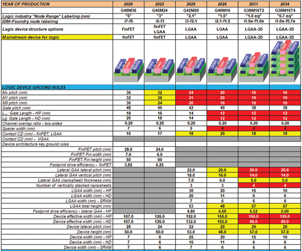
Fig. 6. Key dimensions for the logic technology scaling.
6. 2.5D/3D Integration
Realization of 2D device technologies will enable energy-efficient performance computing, but this will require an architectural adjustment to achieve optimal results. Under these conditions it will be necessary to move the data from the computing logic to the high-capacity memories with high-bandwidth connections. 2.5D systems have already demonstrated to be very efficient in the generations of high-bandwidth memory (HBM) chipsets where stacked DRAM memory cubes (e.g. 128 Gbit/cube) have been put side-by-side in a package with the computing logic die assembled on the same interposer. This technology has demonstrated 64 GB memory with a bandwidth of 2 TB at 512 GB/sec in a single package [7]. In order to keep increasing HBM performance and increasing the total amount of memory in the same package, there will be a need to implement more complex 3D architectures. It is expected that in the next 2‐5 years, work-level memory (e.g. 3D SRAM and/or DRAM on top of logic) will be stacked together on logic to provide a low-latency and large bandwidth communication capability between memory and logic.
Most of 3D stacking technology development focuses on bringing high-capacity memory closer to logic because from a performance point of view it is more advantageous than low-capacity embedded memories and it also offers a better performing bus/IO structure by taking advantage of the better interconnect capability associated with the interposer. In the future it is expected that the interposer technology will allow to place various types of chipsets, (i.e., not limited to memory), in the same package and its fabric would also include voltage regulators, decoupling capacitances, buffers, IO, ESD, etc. There are various implementation routes to enable optimal 3D stacked components. As the combination of 3D stacked components will keep on increasing and as more interconnect routes can be placed on the interposer it will be possible to create larger and larger high performance systems in a single package [9].
Die-to-wafer stacking technologies will continue to employ μBump stacking and/or hybrid/dielectric bonding. Either of those technologies requires Thru-Silicon-Via (TSV) in one or more of the tiers to connect the individual dice stacked onto top of the interposer. Integration drivers for this technology are high-bandwidth and high-density memories stacked on logic die. Furthermore, heterogeneous stacking will be allowing integration of new functions and substantial reduction of form factor. However, design/architecture partitioning, thermal management; and IO and power distribution allocation across the design/system network will still present very difficult challenges. Typical pitch of μBumps on these technologies is presently around 40 μm, enabling 625 vias/mm2, while Cu pad (in hybrid bonding) pitch is around 10 μm, enabling 10,000 vias/mm2.
Wafer-to-wafer stacking is used in applications where there are no issues related to form factor mismatch. This type of stacking was successfully used in image sensors and HBM (stacked DRAM) applications. In this case μBump pitch is around 40 μm while Cu pad (in hybrid bonding) is around 1‐2 μm. Eventually it is expected that this technology could evolve onto the fine-grain and regular fabric suitable for logic-on-logic applications (potentially equalizing the size of different-tier dies) if regular-fabric data-flow micro-architectures will prove successful in the industry.
The technology of sequential integration of multiple tiers of devices relies on the fabricating of subsequent tier using a thermal budget lower than the one used to fabricate any of the underlying tiers. Inter-tier via pitch can be of the order of 50‐300 nm in this technology, enabling 100 M vias/mm2 [10]. It is important to point out that using this integration scheme it becomes possible to independently optimize specific devices in each tier (e.g., threshold voltage, channel material, raised source/drain, strain, etc). Although this technology has many advantages several challenges still lay ahead. Selection of layer-by-layer thermal budgets, integration methodology of high-aspect-ratio vias, selection of cell topology and allocation by layer of interconnection partitioning between fine, median and looser pitch in each tier (e.g. connections between PMOS-tier and NMOS-tier, between standard cells, between standard cell and bitcell) remains a formidable planning challenge. In order to extract the maximum value from this multi-tier architecture it is advisable to select an approach favoring regularity organized layout; this arrangement is ideal to optimize any highly parallel computation and also to accommodate for the fastest memory access while also supporting a very large memory capacity. As time goes by this integrated architecturally driven die layout will make data-centric computing highly successful. It is also possible that this approach may eventually evolve into more general-purpose computing [11]. An example of 3D micro-architecture employing a highly regular layout is shown in Fig. 7; here the sequencer controlling the flow of data across tiers controls computation performance.
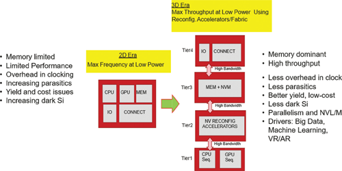
Fig. 7. 3D VLSI enablement with regular fabric.
7. Yield Considerations
In order to be continuing More Moore scaling on multiple layers will necessitate an increased number of metallization layers, therefore the mask count is bound to increase too, barring any new breakthrough in metallization techniques and lithography. The expected transition of multiple challenging mask layers from 193i lithography to EUV, and from EUV (NA = 0.33) to high-NA EUV (NA > 0.5) will potentially save several masks since the desired resolution of lines and spaces can be achieved by a single exposure as opposed to the present situation where 3 or even 4 exposures per layer are required. However, it is expected that the mask count will resume to escalate after 2031 driven by an increased need for metallization layers required by full 3D integration. As the number of layers keeps on increasing so will process complexity and therefore the defectivity (D0) requirements will accordingly become more severe. To keep the yield under control for an 80 mm2 mobile die used as a benchmark for this analysis (Fig. 8) it is necessary that the required D0 level be reduced by 2.2x in 2034 (over 5 logic node transitions)
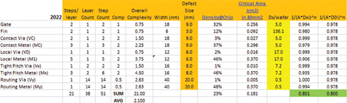
Fig. 8. Critical defect dimension, process complexity, and number of defects/wafer analysis for a projected 3nm FinFET technology to get the initial ramp yield of 80%.
Besides the expected addition of possible defects due to increased process complexity there is also the risk of increased defectivity due to brand new modules causing altogether severe challenges to yields. These are some of the sources of possible defects: smaller defects that were no relevant in the past will become more important as device features keep getting smaller, the number of high-aspect ratio structures such as taller fins and GAA architecture will require more and newer conformal deposition processes, high-aspect ratio contacts will challenge contact and via technologies and control of lateral etch technology and sophisticated sidewall/bottom cleans will be required. In few words there is a concern that the process complexity and the number of materials will increase even though most of the issues are not known at present. Eventually beyond 2030 lithography will no longer be able to resolve some dimensions less than 8 nm or so and overlay requirements of fraction of a nanometer will reach a natural limitation. It is suggested that more reliance on self-organizing structures, self-alignment and self-conformal deposition will be viable by then, but these new process steps will also further increase process and material complexity.
8. Summary of Predictions from 2020 Edition of IRDS More Moore Roadmap
Until approximately the year 2010 personal computers and laptops drove technology requirements. In the past decade mobile devices, cloud data centers, AI algorithms and high-performance computing applications have been driving More Moore scaling requirements. The conditions imposed on transistor performance due to power were limitations and those were partially compensated by the industry with Design-Technology-Co-Optimizaion (DTCO). In the future, Lateral-GAA offers reduced leakage and improved performance at lower operating voltages and it is therefore expected to be a viable path for enhanced PPAC values starting as early as 2022. For the successful deployment of GAA any possible capacitance reduction is a key parameter capable of concurrently resolving performance, power, and thermal issues. For further scalability of power and energy it is estimated that adoption of 2D materials for the channel is a good approach for concurrently reducing both channel length and capacitance. However, GAA manufacturability and contact engineering remain critical challenges to adopting 2D material channel device as a device platform beyond 2028.
Innovative embedded memories technologies are significantly gaining momentum via concrete plans of adopting MRAM and stacked SRAM/DRAM solutions since higher bandwidth and capacity requirements are becoming a major bottleneck that are actually becoming more relevant than solving latency limitations. Nevertheless bandwidth, endurance, and latency improvements are needed to adopt NAND-FLASH as an AI memory solution. Multi-level cell schemes seem to be the preferred route to scale up the number of bits per chip in these memories.
2.5D/3D-stacking technologies are motivated by the benefits of stacking memory-on-logic in large chips such as data servers, AI, and network products as multiple vias of communications between chips are increased (e.g., arrays of bumps). by offering an avenue for products bundling more features and reducing time-to-market. 2.5D integration is expected to continue evolving towards transforming the present passive interposers into active interposers. This approach will enable multi-sourcing and interoperability of various chiplets in the package system whereby the interposer will be providing active and passive functions such as voltage regulation, decoupling capacitances, buffers, IO, ESD, etc.
For more information—visit https://irds.ieee.org/editions/2020.
9. Acknowledgments
The authors acknowledge the IEEE IRDS members for their valuable contributions to the IEEE IRDS More Moore roadmap.
References
[1] IEEE IRDS 2020 edition. Online: https://irds.ieee.org/editions/2020
[2] M. van den Brink, “Continued scaling in semiconductor manufacturing enabled by advances in lithography,” IEDM, December 2019.
[3] S.K. Moore, “A better way to measure progress in semiconductors,” “The node is nonsense,” IEEE Spectrum, August 2020.
[4] C. Auth et al., “A 10nm high performance and low-power CMOS technology featuring 3rd-generation finFET transistors, self-aligned quad patterning, contact over active gate and Cobalt local interconnects,” IEDM, December 2017.
[5] G. Yeap et al., “5nm CMOS production technology platform featuring full-fledged EUV, and high mobility channel FinFETs with densest 0.021 um2 SRAM cells for mobile SoC and high-performance computing applications,” IEDM, December 2019.
[6] M. Badaroglu, “Interconnect-aware technology and design co-optimization for the 5-nm technology and beyond,” Journal of Low Power Electronics (JOLPE), Vol. 14, No. 2, June 2018.
[7] Q Smets, et al., “Ultra-scaled MOCVD MoS2 MOSFETs with 42nm contact pitch and 250uA/um drain current,” IEDM, December 2019.
[8] M. Badaroglu, “3D IC opportunities for high-performance computing”, Semi 3D & Systems summit, January 2020.
[9] A.A. Elsherbini et al., “Heterogeneous integration using omni-directional interconnect packaging,” IEDM, December 2019.
[10] W. Rachmady et al., “300mm heterogeneous 3D integration of record performance layer transfer germanium PMOS with silicon NMOS for low power high performance logic applications”, IEDM, December 2019.
[11] E. P. Benedictis, M. Badaroglu, A. Chen, T.M. Conte, and P. Gargini, “Sustaining Moore's law for 3D chips,” IEEE Computer, Vol. 50, No. 8, pp. 69‐73, August 2017.