Technical Briefs
Beyond CMOS (BC)
Matthew Marinella1, Shamik Das2, Sapan Agarwal1,
Michael P. Frank1, Hiro Akinaga3, An Chen4
1Sandia National Laboratories*, 2MITRE**, 3National Institute of
Advanced Industrial Science and Technology (AIST), 4IBM Research
*Sandia National Laboratories is a multi-mission laboratory managed and
operated by National Technology & Engineering Solutions of Sandia, LLC,
a wholly owned subsidiary of Honeywell International Inc., for the U.S.
Department of Energy’s National Nuclear Security Administration under contract
DE-NA0003525. Approved for public release SAND2021-6396 O.
**Approved by The MITRE Corporation for Public Release; Distribution
Unlimited. Public Release Case Number 20-02213-5.
I. Introduction
CMOS scaling has driven a broad spectrum of applications through increased performance and complexity. As dimensional scaling of CMOS eventually approaches fundamental limits, new information processing devices and architectures have been explored extensively in both academia and industry. The Beyond CMOS (BC) chapter in the International Roadmap for Devices and Systems (IRDS) surveys, catalogs, and assesses viable emerging devices and novel architectures for their long-range potential, and identifies the scientific and technological challenges gating their acceptance by the semiconductor industry. In the previous International Technology Roadmap for Semiconductors (ITRS), the Emerging Research Devices (ERD) chapter covered a similar scope. The BC chapter in IRDS has inherited certain content, structure, and methodology from the ERD chapter in ITRS. During the transition from ITRS to IRDS, the importance of co-optimization of emerging devices and architectures has been increasingly recognized in the broad research community. Therefore, beyond the traditional focus on emerging memory and logic devices, the BC chapter has placed significant emphasis on emerging device-architecture interactions.
Although the semiconductor industry faces difficult challenges in CMOS dimensional scaling, there are promising alternative directions for sustained improvement in chip performance and functionality. Integrating new high-speed, high-density, and low-power memory technologies onto the CMOS platform may break the “memory wall”, improve system performance, and enable new computing paradigms (e.g., in-memory compute). Novel switches based on new materials, alternative mechanisms, and non-charge state variables (e.g., steep-slope transistors, phase-transition devices, nonvolatile switches) may achieve significantly better energy efficiency than CMOS transistors based on thermionic emission over the channel energy barrier. New information processing technologies substantially beyond the capabilities of CMOS may originate from an innovative combination of new devices, interconnect, and architecture for extending CMOS, which may eventually lead to new platform technologies. Ultimately scaled CMOS as a platform technology may also extend into new domain of functionalities and applications (e.g., security, sensing, communication), a general direction known as “more than Moore”. For all these promising directions beyond CMOS and dimensional scaling, new materials and integration techniques play essential roles to enable their implementations.
The BC chapter covers the following major areas: 1) emerging memory and storage devices, 2) emerging logic and alternative information processing devices, 3) emerging device-architecture interactions (including new computing paradigms), and 4) emerging materials integration. This article will briefly review these areas of research and present key observations and recommendations.
II. Emerging Memory and Storage Devices
Memory is an essential element of computing, and the characteristics of the memory device technologies play a significant role in the architecture of an information processing system. A taxonomy of current memory devices is given in Fig. 1. Static and dynamic random access memory (SRAM and DRAM) remain the workhorse computing memory technologies, due to their high speed and endurance. Both are volatile and require backup storage when powered down. Nonvolatile memory includes flash, the most prominent and technologically mature baseline technology. The term “flash” refers to an array architecture for charge based memory cells such as floating gate and charge trapping memory, both of which serve as the main data storage mechanism for most modern information processing systems. SRAM, DRAM, and Flash memory have followed Moore’s Law scaling for several decades, which was tracked by the ITRS until 2015 and is currently tracked by IRDS. Prototypical devices have matured to the point where the technology is in small-scale commercial production, and often the technology is making progress on factors such as scaling and density. In this case, prototypical devices that are making progress have historically been tracked by ITRS and expected future progress is predicted. These technologies include ferroelectric memory (FeRAM), phase change memory (PCM), field-switched magnetic memory (MRAM), and spin transfer torque magnetic memory (STT-MRAM). Several of these technologies, such as STT-MRAM started in the emerging category and have progressed to the prototypical phase and are continuing to progress commercially.
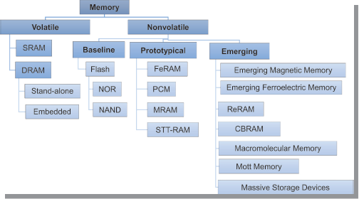
Figure 1. Emerging memory devices taxonomy.
The primary purpose of the Emerging Memory Devices section is to track technical progress for those devices in the rightmost “emerging” column. This section provides a technical overview of each device, and is accompanied by tables that track key properties of these devices as reported in the literature, such as endurance, retention, switching characteristics, and minimum dimensions. These emerging memory devices are the subject of significant research, with potential to continue storage density scaling beyond physical limits of flash, improve computing efficiency by enabling storage class memory, and enable new computing paradigms such as in-memory compute.
One of the most active emerging memory research topics is magnetic memories. STT-MRAM has made significant progress in the past decade, and recently we have seen the emergence of several commercial products and integration in commercial foundries. This is due to excellent scalability, CMOS-compatible voltages, high endurance, and compatibility with back end of line CMOS processes. STT-MRAM has the potential for future use as a cache replacement, [1] although it will be important to reduce switching current, increase speed, and increase energy efficiency. This need for improved magnetic memory properties has prompted research in emerging magnetic devices. One example is the three terminal memory structure which harnesses spin orbit torque (SOT) effect, reducing the current density required to switch the magnetization of a magnetic tunnel junction (MTJ). Another active area of research is in voltage controlled magnetic anisotropy (VCMA), which harnesses magnetoelectric effects to reduce the energy and improve the speed of MTJ switching [2].
Resistive and conductive-bridge random access memory (ReRAM and CBRAM), have seen also significant commercial interest and research activity in the literature, due to potential for applications such as storage class memory, edge computing, and efficient processing of neural networks. These are two terminal resistive switching device structures, with a memory state defined by the resistance. This resistance is controlled by the connecting and breaking of metallic conductive filaments (CBRAM) or modulation of oxygen vacancy concentrations in a metal oxide (ReRAM). Resistive memories are highly scalable and CMOS-compatible, and hence are being integrated into foundry processes. Research challenges for these devices continue to be improving the understanding, parametric control, and reliability. Emerging polymer memories, which incorporation organic materials, often rely on similar physical mechanisms to ReRAM and CBRAM [3].
Ferroelectric memories, including the ferroelectric field effect transistor (FeFET) have seen a resurgence of interest recently due to the discovery of ferroelectricity in HfO [4] which has provided a path for FeFET scalability and CMOS compatibility. Other new technologies that are further from commercialization (and lack concrete benchmarks) have become the subject of significant research. For example, DNA storage (covered under massive storage devices) has the highest volumetric information storage capacity of any known medium, which has motivated research to tackle the practical challenges of using these complex organic molecules for information storage. It is hoped that the IRDS coverage of emerging memories can serve as a reference for the electron device community and engineers in understanding new memory devices and their impact on future computing systems, for funding agencies in understanding the memory research challenges, as well as for students and others in academia who need a better understanding of the memory research landscape.
III. Emerging Logic and Information Processing Devices
For nearly twenty years, the industry’s semiconductor roadmap has featured device options that might surpass silicon CMOS as the driver for logic, computation, and information processing applications. Originally captured as Emerging Research Devices, recent editions of the IRDS present these as Logic Devices Beyond CMOS. Though silicon CMOS has proved exceptionally hardy and productive over the last twenty years, the roadmap continues to track Beyond-CMOS devices for both near-term successors and more disruptive, longer-term candidates.
Figure 2 depicts the taxonomy of emerging logic devices as conveyed in the IRDS. Such devices depart from the present state-of-the-art in two primary ways. First, the structure and materials constituting the device will be different to some degree from silicon planar FETs or FinFETs. This departure is shown on the horizontal axis. Second, the physical manifestation of digital information, also known as the state variable, may differ from the electric charge that is used in FETs. This is shown on the vertical axis. Considering these elements together, a natural three-part grouping emerges that is used to characterize near-term vs. far-term candidates for the evolution of semiconductors.
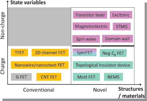
Figure 2. Taxonomy of logic devices beyond CMOS. Reproduced from Figure BC3.1 of the 2021 IRDS Beyond CMOS chapter.
The nearest of these candidates are the conventionally structured, charge-based devices listed in the lower left of the figure. Such devices include nanowire transistors and carbon nanotube transistors, for example. The intent with these devices is to obtain charge transport characteristics exceeding the semiconductor channels of conventional devices. Thus, a few of these candidates could be considered as potential channel-replacement technologies for near-future state-of-the-art devices and are also tracked within the “More Moore” component of the IRDS. This includes “stacked nanosheet” devices as well as vertical gate-all-around (VGAA) transistors.
Further evolutions of charge-based devices are considered in the lower right of the figure. Here, one begins to see mechanisms for modulating charge transport that differ from the electrostatic field effect. Some examples include using a type of metal-insulator phase transition (Mott transition) as a switch or using electromechanical potential to store a digital state. Because of the greater departure in materials systems from CMOS as compared with the first category of candidates, it is expected that integration with CMOS will be more complicated and take longer to manifest commercially. Also, it is less clear for any of these devices that there is a route to the kind of universal performance applicability and scalability that has made silicon CMOS economically viable for so long.
A recent addition to the Beyond CMOS roadmap in this second group of the figure is the topological insulator transistor. Research into topological insulators as materials has increased substantially in recent years, primarily for applications in quantum information science. Some of these research results suggest routes to using topological properties to increase the speed and power efficiency of field-effect devices. It is an ongoing line of inquiry to determine if such advantages can be materialized robustly at room temperature with commercially relevant yields.
Finally, the Beyond CMOS roadmap has always monitored the progress in devices shown at upper right in the figure, which represent a substantial departure both in form and function from conventional semiconductor field-effect transistors. Principally, these devices use a non-charge-based state variable, such as a remnant magnetization, exciton, or optical/photonic state. In some cases, state information can be transported via charges, such as with a spin-filtered electronic current. In others, the change in state variable also requires a novel form or material structure for the interconnect. Thus, development and commercial maturation for these candidates is expected to take significant time, or else such devices might only be used within heterogeneous integration contexts, i.e., alongside state-of-the-art silicon.
As the industry progresses and the nearer-term Beyond CMOS candidates become more central to the IRDS, the focus of logic device evaluation beyond CMOS will evolve. Though the core focus remains on digital information processing, it seems less and less likely that a candidate will emerge that will take over the mantle of the silicon FET as the workhorse of linear, multi-generational progression for the industry. Instead, a variety of devices tailored to a variety of applications and accelerators will need to be explored and matured using ultimate silicon as a foundation for experimentation and commercialization.
IV. Emerging Architectures and Device Interaction
Many new emerging devices will require co-design between devices and higher levels of computer design (e.g., circuit, architecture, and application). These emerging devices are not intended simply as “drop-in” replacements for standard CMOS devices, but will require new types of circuit designs, new functional module architectures, and even new software to best utilize the new devices’ capabilities [5].
Novel design issues that span the device and architecture levels especially need to be considered when adopting new low-level computing paradigms. Devices may be organized in radically new ways to carry out computation in a very different style from what we may consider the most “conventional” computing paradigm, which has relied on standard combinational and sequential non-reversible Boolean logic. The Beyond CMOS roadmap has begun tracking some of the most common building blocks for emerging systems and applications as shown in Fig 3.
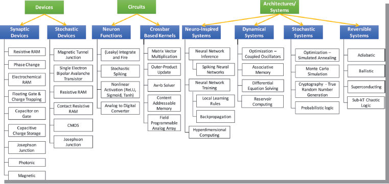
Figure 3. Emerging architectures require co-designing new devices, computational kernels and computational systems. Some of the possible building blocks are shown.
At the device level, there are many types of devices that function as a synaptic device that both hold a stored state and use that state to modulate an analog input. This type of device is critical to overcoming the von Neumann Bottleneck: rather than moving data between memory and a processor, processing is directly integrated with each memory element. The analog processing of a synaptic device can also replace the 1,000’s of transistors needed to do a digital operation with a single device. Another important class of devices are stochastic devices that generate a random binary or analog value. For many of the devices the probability distribution is tunable allowing for controllable randomness. Conventional digital logic is deterministic and cannot introduce true randomness, and instead require relatively expensive pseudo random number generators (PRNGs). Replacing a large expensive PRNG with a single device allows one to consider algorithms that are inherently stochastic and would otherwise be computationally expensive.
At the circuit level there are both circuits dedicated to computing a specific “neuron” function very efficiently, and circuits that are based on a crossbar array of synaptic devices to compute a given matrix operation. Converting between analog and digital is typically a very expensive operation, and so neuron devices and circuits that can directly operate on an analog input avoid this cost. Common functions include leaky-integrate-and-fire neurons, stochastic spiking neurons, rectified linear neurons, and sigmoidal neurons. At the array level, there are computational kernels that can read a matrix in parallel by performing matrix vector multiplication, write a matrix in parallel by updating all values by the outer product of two input vectors, approximately solve the matrix equation Ax = b for a vector x, implement a content addressable memory, and provide a reconfigurable analog computing substrate through a field programmable analog array.
These enabling devices and circuits can then be used to build a wide variety of architectures and systems. Neuro-inspired systems include conventional neural network inference and backpropagation based training. Spiking neural networks promise to reduce communication and analog to digital conversion (ADC) costs. New neural training algorithms based on local learning rules promise to drastically reduce the data-movement and buffering needed to train a neural network. Hyperdimensional computing is a new high-dimensional learning system that is enabled by large hardware-based content addressable memories.
Dynamical systems can use the temporal evolution of a recurrently connected system to solve a variety of problems. Coupled oscillators can be used to solve optimization problems. Associative memories can be stored in Hopfield networks. Differential equations can be mapped to analog substrates, and reservoir computing systems can be used to analyze temporal data. Chaotic logic networks can carry out monolithic reversible transformations of the state of a Boolean circuit even down to sub-kT signal levels.
Stochastic devices enable new systems that are built around repeated random sampling. Simulated annealing can be used to solve optimization problems. Stochastic devices enable Monte Carlo simulation. True random number generation is critical for cryptographic applications and tunable random devices enable probabilistic logic.
In addition to developing accelerators for specific computing functions, reversible computing systems aim to lower the energy dissipation of general digital logic, including both general-purpose programmable digital processors, and more specialized digital ASICs. Rigorous thermodynamic arguments have shown that the fundamental Landauer limit on energy efficiency can only be avoided in deterministic computational processes composed from local primitive operations if they have the property of (conditioned or unconditional) logical reversibility [6]. In addition to the potential for reducing minimum energy dissipation below conventional limits, reversible techniques can potentially exceed the conventional limits on larger-scale practical computing efficiency. Concrete examples of reversible computing systems based on both semiconducting and superconducting technology platforms have been demonstrated, and this area seems ripe for further development.
In this section, the Beyond CMOS roadmap has surveyed a variety of concepts and R&D directions for the development of novel beyond-CMOS computing technologies that represent an effort to think “outside the box,” in the sense of looking beyond just developing simple drop-in replacements for traditional logic and memory cells. More broadly, new hardware designs spanning multiple levels from the devices up through circuits and architectures must be considered, and the interactions between the various levels explored. More specifically, we expand the scope of future computing technologies beyond traditional irreversible, deterministic digital logic to include a broad range of alternative, unconventional computational paradigms, such as analog, probabilistic, and (classical) reversible computing paradigms.
V. Emerging Materials Integration
In the previous ITRS activities that form integrated knowledge and collective intelligence in academia, consortia, and industry researchers, the international technology working group of Emerging Research Materials (ERM) presented potential solutions from a materials science perspective for future logic and memory devices, front end processing, interconnects, assembly and package, lithography, metrology, and life-cycle assessment of Environment, Safety, and Health (ESH)-related issues [7]. Taking over that experience, the IRDS 2020 edition set up “Emerging Materials Integration (EMI)” section in the “Beyond CMOS” chapter. While existing technologies are integrated on a Si-based platform, the majority of beyond-CMOS technologies are based on entirely new materials and cutting-edge material science. The key EMI challenge is to provide timely guidance on emerging materials, process performance, cost, reliability, and sustainable developments that will drive breakthroughs in the future. Figure 4 depicts the role of EMI, which is to promote the advancement of existing technologies.
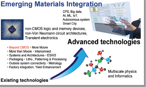
Figure 4. Emerging Material Integration promotes the advancement of existing technologies.
The current EMI section emphasizes strategic challenges, novel breakthroughs, and potentially disruptive opportunities for emerging material properties, synthetic methods, and metrology, organized in the following areas: (1) Scaled technology materials needs for More Moore, (2) Novel materials for Beyond CMOS, and (3) Potentially disruptive material opportunities for functional scaling and convergent applications. Regarding materials for advanced More Moore technologies, high mobility transition metal dichalcogenides (TMD) with low defect density and low resistance ohmic contacts are listed as a long-term difficult challenge. Nano-carbon materials, complex metal oxides and spin-related materials are attracting attention as materials for non-CMOS logic and memory devices. Novel interlayer dielectrics, such as Metal Organic Framework (MOF) and Carbon Organic Framework (COF) will improve the interconnect reliability. Materials and processes that enable monolithically 3D integrated complex functionality, such as integration with flexible electronics and biocompatible functional materials, are also included in long-term challenges. As one of the convergent opportunities, EMI section refers to Big data and Digital transformation (DX) issues. Robust and ubiquitous information processing and independent power supplies (such as Energy Harvesting expanding the IoT utilization, one of the major topics in “More than Moore” chapter) will be a place for emerging materials to play an active role. Emerging materials have been spurring developments of non-von Neumann architectures for novel computing, such as neuromorphic computing, reinforcement learning, topological quantum computing, reversible computing, and probabilistic computing. A typical example is physical reservoir computing. Since computing performance in these systems depends on the unique material properties of the reservoir, the material research to optimize physical phenomena for reservoir computing will directly improve performance metrics such as energy efficiency. It is expected that the output of energy harvesting and the required power for novel computing approaches will be matched in the near future.
To drive emerging material technologies, the EMI section focuses on multiscale simulation. Conventional multiscale physics modeling was described previously in the ERM chapter of ITRS, where the physics to explain mesoscopic level phenomena is required to link electronic properties and device characterization. In the EMI section of the current BC chapter, a potential role for machine learning and informatics has been suggested as an alternative to the simulation in the mesoscopic level, where inputs of molecular level phenomena provide an output describing continuum level phenomena. Transient electronics is introduced as one example of a disruptive technology. Here, materials, devices, and systems disappear with minimal or non-traceable remains in a controllable period of time. The spontaneous and transient functions in the material property, such as a conductance change with a controllable decay in atomic switches, are also treated with the appearance of transient electronics in the EMI section. This emerging electronics with a ‘fading’ capability will bring about intelligent applications, such as environmentally friendly electronics for one of the targets of SGDs Goal 12, to substantially reduce waste generation through prevention, reduction, recycling and reuse [8]. Future editions of EMI will provide additional descriptions and continue to adapt its scope to engage with societal environment, such as autonomous systems, smart cities and CPS. Cooperation with international standardization groups, which prepares a common protocol for assessing the properties of emerging materials, will also be considered part of EMI activities.
VI. Assessment
With a large variety of mechanisms and characteristics as well as different levels of maturity, beyond-CMOS devices present a unique challenge for assessment of their performance and potential. The BC chapter has referenced the emerging device benchmarking in the Nanoelectronics Research Initiative (NRI) for quantitative assessment [9]. The NRI benchmarking evaluates novel switches in conventional Boolean logic circuits (e.g., an inverter, a 2-input NAND gate) with quantitative metrics (e.g., speed, power dissipation, footprint, span of control, logical effort). Although the assessment of beyond-CMOS devices is an evolving effort and conclusions could be continuously altered by new research progress, some observations are worth noticing. First, the power-speed tradeoff commonly observed in CMOS continues to be a challenge for beyond-CMOS devices. Many beyond-CMOS devices utilize novel mechanisms and non-charge state variables to achieve low switching power; however, communication with many non-charge tokens is often significantly slower than moving charges. Second, most beyond-CMOS devices have not been shown to be capable of replacing CMOS with better power-speed performance. CMOS will remain the primary basis for IC chips for the coming years. Some promising beyond-CMOS technologies could be utilized to augment CMOS as special purpose accelerators to offload specific computations from the general-purpose processors. While integrating dissimilar technologies and materials is challenging, advance in heterogeneous integration may make this more feasible over time. Third, as the characteristics of beyond-CMOS devices become better understood and controlled, work on novel architectures that can leverage these unique devices becomes increasingly important. Co-optimization of emerging devices and architectures may have great potential to improve the energy efficiency and performance of computing systems. Last, the high-precision fabrication capabilities critical to CMOS (e.g., patterning, deposition, purity, doping, alignment) will continue to be important in the realization of systems built upon beyond-CMOS devices.
Previously, the ITRS ERD chapter utilized a survey-based critical review to assess the potential of beyond-CMOS devices, as a consensus among researchers participating in the survey. The ERD assessment measured devices on a scale of 1 to 3 on a set of criteria, including scalability, speed, energy-efficiency, gain (or on/off ratio), operational reliability, operational temperature, and CMOS compatibility. A spider chart was used to visualize the assessment. The ERD survey-based assessment has been widely cited in literature, although the scale of the survey sometimes raised questions about the accuracy of some assessment. At the same time, for highly exploratory devices without sufficient data, this assessment based on the survey of experts’ perspective indeed provided an alternative measure of their potential.
As beyond-CMOS devices are being developed increasingly for novel computing paradigms beyond Boolean logic and von Neumann architecture, benchmarking cannot be simply performed at the device or logic gate levels. Benchmarking across multiple layers from devices to architectures is a great challenge that has to be addressed by interdisciplinary collaborations. Facing a large variety of design options and applications, benchmarking needs to be focused with well defined criteria and assumptions in order to produce meaningful results. Unlike in mature technologies where benchmarking may be more conclusive, beyond-CMOS benchmarking may provide guidance more than drawing definitive conclusions.
VII. Summary
Beyond-CMOS research has gone through a transition from a focus on novel devices with the potential to replace CMOS transistors to a holistic approach driven by device-architecture interaction and cooptimization to augment CMOS. The IRDS Beyond CMOS (BC) chapter not only tracks the progress of emerging logic and memory devices but also summarizes their utilization in unconventional computing architectures and applications. New computing paradigms may exploit unique characteristics of beyond-CMOS devices for more efficient native implementations of key functions. These promising devices often rely on emerging materials and advanced fabrication and integration techniques for demonstration and prototyping. The IRDS Beyond CMOS (BC) chapter covers promising research directions from materials and devices up to designs and architectures, to provide a comprehensive reference for research beyond conventional CMOS technologies, Boolean logic, and von Neumann architectures. As the dimensional scaling reaches its limits, continued improvement of chip efficiency and performance may be driven by co-optimization, integration, and functional diversification. Beyond-CMOS devices and architectures may provide promising technology options for ongoing improvement.
References
[1] G. Hu et al., “Spin-transfer torque MRAM with reliable 2 ns writing for last level cache applications,” 2019 IEEE International Electron Devices Meeting (IEDM), pp. 2.6.1–2.6.4 (2019). doi: 10.1109/IEDM19573.2019.8993604
[2] B. Rana, Y. Otani, “Towards magnonic devices based on voltage-controlled magnetic anisotropy,” Communications Physics 2, 90, pp. 1–12 (2019). doi: 10.1038/s42005-019-0189-6
[3] Q.-D. Ling, D.-J. Liaw, C. Zhu, D. S.-H. Chan, E.-T. Kang and K.-G. Neoh, “Polymer electronic memories: materials devices and mechanisms”, Progr. Polymer Sci., 33, pp. 917–978 (2008). doi:10.1016/j.progpolymsci.2008.08.001
[4] T. S. Böscke, J. Müller, D. Bräuhaus, U. Schröder, and U. Böttger, “Ferroelectricity in hafnium oxide thin films,” Applied Physics Letters, 99(10), p. 102903 (2011). doi: 10.1063/1.3634052
[5] T. P. Xiao, C. H. Bennett, B. Feinberg, S. Agarwal, and M. J. Marinella, “Analog architectures for neural network acceleration based on non-volatile memory,” Applied Physics Reviews, 7(3), p. 031301 (2020). doi: 10.1063/1.5143815
[6] M. P. Frank and K. Shukla, “Quantum foundations of classical reversible computing,” Preprints (2021), 2021050066. doi: 10.20944/preprints202105.0066.v2
[7] S.W. King, H. Simka, D. Herr, H. Akinaga, and M. Garner, “Research updates: the three M’s (materials, metrology, and modeling) together pave the path to future nanoelectronic technologies,” APL Materials, 1, p. 040701 (2013). doi: 10.1063/1.4822437
[8] United Nations Development Programme: GOAL 12 TARGETS [Internet] (accessed April 20, 2021) (https://www.undp.org/content/undp/en/home/sustainable-development-goals/goal-12-responsible-consumption-and-production/targets.html)
[9] C. Pan and A. Naeemi, “An expanded benchmarking of beyond-CMOS devices based on boolean and neuromorphic representative circuits,” IEEE J. Exploratory Solid-State Computational Devices and Circuits 3, p.101 (2017). doi: 0.1109/JXCDC.2018.2793536
Your Comments Solicited
Your comments are most welcome. Please write directly to the Editor-in-Chief of the Newsletter at daniel.tomaszewski@imif.lukasiewicz.gov.pl