Technical Briefs
Marvels in Process Technology Before and During Moore’s Law Era
By Joachim N. Burghartz, Institut für Mikroelektronik Stuttgart
(IMS CHIPS), Germany
Process technology has always been the guiding and decisive factor in keeping Moore’s Law going. Since the 1980’s, the semiconductor roadmap helped us looking at the processing needs ahead—this was well coordinated ‘engineering on demand’ by semiconductor manufacturers, equipment vendors and academics with countless brillant efforts and results on the way. However, there were also marvels in process technology that came out of the blue or with an impact that was not foreseen at all. This third article of the series on ‘Marvels of Microelectronics Engeneering’ will highlight a few of those.
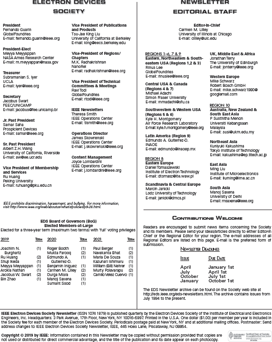
One might think that in the years before Moore’s Law was formulated technology progress in semiconductors was solely based on marvellous discoveries. According to Adolf Goetzberger, former director of the Fraunhofer Institute for Applied Solid State Physics and retired founding director of the Fraunhofer Institute for Solar Energy Systems in Freiburg, Germany, this was, however, not the case in the old days. Goetzberger worked with Shockley from 1958 to 1963 after in 1957 the ‘Traitorous Eight’ left Shockely Laboratories in Palo Alto. In my recent personal conversation with him he rememberd about Shockley: “We had agreed that I would be in charge of the experiments and he would do the theory. This turned out to become a very good collaboration”. Apparently, the theoretical work by Shockley came first and experiments followed to demonstrate the theories. This approach might have been triggered by Shockely’s personal experience from the demonstration of the first transistor by Bardeen and Braittain in 1947; it was just after the transistor was demonstrated experimentally that Shockley could complement that birth of semiconductors by his transistor theory.
Former Shockley Laboratories in Palo Alto (left) and Adolf Goetzberger, research staff at Shockley Labs in the 1960‘s (Images provided by Adolf Goetzberger)
However, also at Shockley Labs there were instances where experimental success came first. Goetzberger: “In the old Labs in San Antonio Road, diffusion furnaces were set up in a former barn. We did not know about clean work conditions. The pn junctions we fabricated were generally not ideal. More or less by accident, but also by my structured follow-up on observations and reproduction of experiments, I found a technology which gave us perfect junctions every time. This is the gettering step which has been customary in semiconductor technology for several decades”. Goetzbergers discovery of metal gettering is a true marvel in semiconductor process technology. He and Shockley published this in the Journal of Applied Physics in 1960. For many years highly doped p-type silicon wafers with lower doped epitaxial device layers had been used to getter metal precipitates and achieve ideal pn junctions. Adolf Goetzberger received the 1983 J.J. Ebers Award in honor of this achievement.
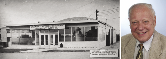
While Goetzbergers discovery was accidental and provided a solution to a known problem, another great invention in microelectronics—the sidewall spacer—showed up as an artifact of anisotropic dry etching. Etching in a gaseous atmosphere instead of in liquid chemicals gained attention when both more accurate transfer of lithographic pattern and high selectivity to underlying layers became crucial. In 1975, Texas Instruments demonstrated the first all-dry-etched device, a CCD shift register. However, with the anisotropic nature of the so-called reactive ion etch (RIE) a problem arised: film removal at a steep sidewall became very difficult; only a substantial overetch could remove the undesired residues. It took about five years until Bernie Pogge at IBM thought of making use of this previously undesired sidewall feature. In 1981, he filed US patent 4,256,514 in which he decribed that sidewall to be used as a lateral spacer with its dimension being controlled by the thickness of the previously deposited film. IBM Fellow Tak Ning remembers: “Once the concept was out, many companies explored using sidewall spacer to improve devices or to come up with novel device structures”.
Schematic illustration of the sidewall spacer from Bernie Pogge’s US Patent 4,256,514 (left) and SEM cross section of a MOS gate with an LDD spacer (middle), and Tak H. Ning, inventor of the double-poly self-aligned bipolar transistor (right). (Images from J.N. Burghartz, “Guide to State-of-the-Art Electron Devices,” Wiley)
First was Ning’s invention of the double-poly self-aligned bipolar transistor which he presented in a Late News paper at the 1980 IEDM. He placed a sidewall spacer inside the lithographically defined emitter window and, thus, achieved a sub-lithographic emitter leading to a much reduced intrinsic base resistance. The sidewall also provided a self-aligned isolation of the emitter polysilicon contact to the extrinsic base polysilicon. Ning’s double-poly self-aligned bipolar transistor became a standard in semiconductor industry and—in its general form—is still in manufacturing, though today with an epitaxial SiGe:C rather than an implanted Si intrinsic base (see EDS Newsletter Ocober 2018). Tak Ning received the 1989 J.J. Ebers Award partly for his pioneering contribution to bipolar technology.
Next was the lightly-doped drain (LDD) structure using source/drain implants before and after formation of a sidewall-spacer around the gate contact of a MOS device. Ning: “Seiki Ogura’s LDD concept was reported in 1981 at IEDM. It was quite effective in suppressing the hot-carrier effect, but only for 5 V designs. Once voltage was scaled down to 2.5 V hot-carrier effect was no longer an issue, and LDD was no longer needed. I would say that LDD was used in high-speed CMOS logic for less than 10 years by the industry”.
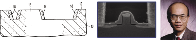
Burn Lin, inventor of immersion lithography (left), schematic of practical implementation of immersion lithography in a commercial step-and-repeat equipment (right)
Another application with high impact was the self-aligned silicide (salicide) process introduced by a team at Texas Instruments, which provides self-aligned metallization at the source, drain and gate contacts of a MOS transistor. The late Roger A. Haken, in whose memory the IEDM named its Best Student Paper Award, was a member of that pioneering team. They published this breakthrough in the 1985 February issue of the IEEE Transactions on Electron Devices.
The sidewall spacer also affected the art of lithographic patterning in different ways. In the 1970’s, that was used to form a sub-lithographic feature, e.g. a gate contact of a MOSFET. The dummy feature, at which the sidewall spacer was formed and which was removed later on, was called mandrel. Since the sidewall spacer was formed around the mandrel, it had partly to be etched off. This technique was known as sidewall image transfer (SIT). The interest in SIT disappeared with the progress made in lithography but SIT returned in recent years with use in double- and multiple-patterning.
Progress in photolithography was often based on concerted engineering actions but in a few cases innovations appeared as true marvels. Photolithography was introduced in 1958 by Lathrop and Nall from Army Research Laboratories in the US. It became an integral part of the planar process technology, invented by Jean Hoerni in 1957, and the planar integrated circuit, invented by Bob Noye, both with Fairchild at that time and two of those Traitorous Eight whose sudden leave brought Adolf Goetzberger to Shockley Labs.
Tim Brunner, a Globalfoundries Fellow, who spent his professional life in photolithography, mentiones a few milestones: “The chemically amplified photoresist process, invented in late 1980’s by Grant Willson and Hiroshi Ito, was essential to high volume manufacturing for three decades. Step-and-scan exposure tools, invented by Perkin-Elmer/SVG in 1973 and then perfected by Nikon and ASML, advanced data-preparation methods, such as Optical Proximity Correction (OPC) and Sub-Resolution Assist Features (SRAF), and computational lithography methods like Source Mask Optimization (SMO) need to be mentioned”. He also points to Extreme Ultra Violett (EUV) lithography as an “incredible engineering tour-de-force that will soon emerge as production-worthy”. To him, however, “193 nm immersion lithography was a true marvel that came out of the left field to defeat the crappy 157 nm exposure technology”.
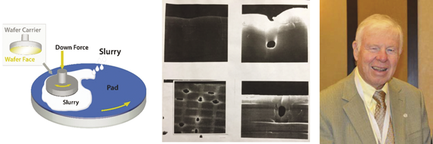
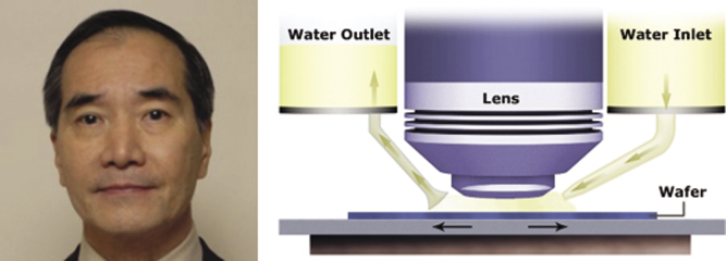
Schematic illustration of chemical-mechanical polishing (CMP) (left), images from the first device experiments (middle) and CMP inventor Klaus Beyer (right). (Photographs provided by Klaus Beyer)
Immersion lithography, using water instead of air between lens and wafer, was introduced in 1987 by Burn Jeng Lin, then at IBM, at the Microcircuit Engineering Conference on the future of subhalf-micrometer optical lithography. He remembers: “In that presentation, I told the audience that immersion lithography would be a way to extend optical lithography. There was no immediate follow up because there were many easier ways to extend optical lithography”. Lin further: “By 2002, the wavelength has been reduced from 436 nm to 365, 248, 193 and heading to 157 nm. The numerical aperture of the imaging lens had been increased from 0.18, through many steps, to 0.93. Most resolution enhancement techniques had been implemented. That is: unwanted reflections and vibrations in the imaging system have been managed, phase shifting masks were used, off-axis illumination was implemented, and optical proximity correction was introduced. We were facing the limit of Moore’s law scaling at the 65 nm logic node and could at most stretch to the 55 nm half node. Reducing the wavelength to 157 nm seemed to be the last resort to improve the resolution but that ran into tremendous difficulties”. Burn Lin explains further: “My solution to the above problems was to stay away from the 157 nm wavelength. The vacuum wavelength of 193 nm light becomes 134 nm in water due to its refractive index of 1.44 at the 193 nm vacuum wavelength. This wavelength is much shorter than 157 nm and can keep the entire optical train in 193 nm. This includes the light source, the illuminator, the mask, the pellicle, the imaging lens, and the environment. One only has to keep the space between the last element of the imaging lens and the photoresist immersed in water and the actinic wavelength will be 134 nm. This configuration is, of course, immersion lithography. At that time the entire lithography community including suppliers and users were all concentrating on making 157 nm work. One billion dollars was estimated to have been spent on this effort”. Lin, who was 16 years with TSMC, as senior director and vice president, remembers: “A more difficult task followed. We had to turn the industry around from 157 nm conventional to 193 nm immersion, technically, politically, and commercially”. Burn Lin received the 2013 IEEE Jun-Ichi Nishizawa Medal for his pioneering work and his leadeship in immersion lithography.
Immersion lithography turned out to carry the 45 nm, 40 nm, 32 nm, 28 nm, 20 nm, 16 nm, 14 nm, 10 nm, and 7 nm nodes in a span of about 12 years. Besides immersion, also those many other ‘tricks’ mentioned have to employed to arrive at such small dimensions. One of those extras is double- and multiple patterning, taking advantage of patterning two or more masks to reduce the combined pitch or the SIT enabled by the sidewall spacer, the other marvel in microelectronics we mentioned. This is not the only entanglement of marvellous inventions in microelectronics.
Photolithography also has a close relationship with another marvel in microelectronic engineering, i.e. chemical-mechanical polishing (CMP). This process is applied numerous times in the course of circuit integration to return to a perfectly planar wafer surface. This allows to arrive at an optimum resolution in a trade-off against a small depth-of-focus (DOF).
CMP on device structures was invented by IBM Fellow Klaus Beyer. Beyer was assigned by his manager the task of finding a way to eliminate silicon wafer surface scratching caused primarily by the traditional brush cleaning method used to remove the colloidal silica polishing slurry. In the course of his investigations Beyer started to successfully use megasonic cleaning to remove those residues. In a personal communication Klaus Beyers said: “The first CMP application to silicon surfaces was achieved by Walsh and coworkers at Monsanto Corp. in 1962. Approximately in 1973 Monsanto engineers installed their CMP process at IBM. On March 20, 1983, at the 1983 American Chemical Society Meeting in Seattle/Washington, I showed voltage breakdown measurements of oxides grown on silicon surfaces cleaned by megasonic cleaning of colloidal silica covered silicon surfaces. I mentioned the possibility of this process for device applications”. About 12 months earlier he was approached by a development manager and asked to also work on trench refill using glass reflow. His then two managers made a deal and had him work half-time on each of those tasks. At 1.5-µm trench width the glass trench refill process caused unwanted mounds after reflow at random locations. Out of desperation, on a day in January 1983 Klaus Beyer applied his meanwhile scratch-free polishing process from his other job assignment with the result that the device structures became perfectly planar. This was the birth hour of CMP on device structures. Beyer remembers the difficulties they had at IBM before CMP was applied to multi-level interconnects: “A very important problem was also the wiring of computer chips. The extension from three- to four-level wiring was very difficult. Planarization of interlevel oxides was done by applying photoresist as a planarization medium with a subsequent RIE etch-back. However, this only worked for certain layout configurations.” In 2002, Klaus Beyer retired from IBM after having received a major invention award fom IBM’s CEO Lou Gerstner, and in 2015, he received a Lifetime Achievement Award from the International Conference on Planarization/CMP Technology (ICPT).
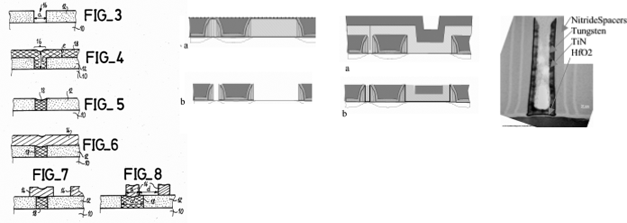
Contact/Via plug principle: detail of France/EU patent: 84.05906 (US patent #: 4,592,802) filed on April 13, 1984 by Simon Deleonibus and Guy Dubois, for Thomson Semiconductors (now ST Microelectronics) (left). First publication of totally self aligned damascene metal gate last/ HiK CMOS integration at IEDM 2002 by CEA, LETI and STMicroelectronics (3 images on right side). (Images provided by Simon Deleonibus)
CMP was also instrumental in enabling Cu damascene, optimized tungsten contact/via plug formation in aluminum multi-level interconnects in the 1990’s and to realize metal replacement gates in the 2000’s. The plug concept goes back to work at ST Microelectronics in 1983/84 by IEEE Fellow Simon Deleonibus and Guy Dubois. Simon Deleonibus explains: “I was hired by Thomson Semiconductors in 1981, after my PhD. We tried to increase, as much as possible, the step coverage of sputtered or evaporated aluminum in high-aspect-ratio contacts to avoid high contact resistance and reliability issues. We tried several solutions to smoothen the contact opening topography and came to the conclusion that refilling the contact with a metal by a conformal deposition would solve both step coverage and reliability problems. We filed the basic generic patent on the contact/via plug principle in early 1984 (France/EU patent: 84.05906, US patent 4,592,802). Our patent covered any conformally deposited metal and any type of removal process. It also offered to reduce the metal levels contacted pitches. I joined CEA, LETI in 1986 and continued my work with my colleagues there. Finally, we published the contact/via plug for 16Mb EPROM at IEDM 1989, featuring W as refill material, TiN/Ti barrier/contact metal stack. W and TiN/Ti were smoothened and etched back by RIE at that time. CMP of W was applied much later by the mid 1990s when the cost-of-ownership was less an issue in synergy with interlevel dielectric planarization and later on Cu integration. The whole microelectronics business is using the plug principle at the sub-10 nm level and has extended it to Through Silicon Vias (TSV). The French Academy of Technologies awarded me with their 2005 Grand Prix for the invention and development of the plug principle, a major innovation for the industry”.
Simon Deleonibus continues: “By 1995, I started to develop the damascene metal-gate-last integration. The plug principle was of great inspiration to apply a low thermal budget process on the metal gate material. Annealing before metal deposition was necessary to self-align sources and drains to gate, protect salicided junctions from degradation, keep the metal workfunction value stable and avoid any reaction with the underlying gate dielectric. In 1996, I and François Martin, both with CEA, LETI, filed the patent (France/EU patent 96.15436, US patent 6,346,450) showing the way to integrate the gate-last metal with total self alignment, thanks to the use of a replacement material and the planarization of the final metal by CMP. We published the first results using a W/TiN/HiK(Hf02 deposited by Atomic Layer Deposition) gate stack at IEDM 2002. Today, the damascene gate is massively used by Intel and other manufacturers!”.
The gettering technique, the sidewall spacer with its impact on self-aligned bipolar technology, LDD, sacilide and lithographic multiple patterning, immersion lithography, CMP and the via/contact plug principle with extension to damascene gate are true marvels in semiconductor process technology. They all had tremendous impact on keeping Moore’s Law to go on.
Your Comments Solicited
Your comments are most welcome. Please write directly to the
Editor-in-Chief of the Newsletter at
clilley@uic.edu