Marvels of Microelectronic
Engineering

Joachim N. Burghartz |
Simon Deleonibus |
We look back at 50 years of microelectronics initiated through the famous prediction by EDS Celebrated Member Gordon Moore in 1965. Since 1992, semiconductor manufacturers, equipment suppliers, research institutes and peripheral stake holders have been sitting at the table to make concerted actions towards what is needed to fulfill the technological requirements ahead, with the semiconductor roadmaps as the result. |
| Microelectronic engineering became predictable and was less based on surprising discoveries, as in the pioneering years prior to Moore’s Law. However, throughout the Moore’s Law era there were still unexpected discoveries, underestimated applications and underrated impacts of electronic materials, process technologies, device structures, techniques and semiconductor technologies, which helped advancing microelectronics in a remarkable way. Coincidentally, the techniques that microelectronic engineers and scientists developed inspired their colleagues in other fields to miniaturize functions that were not expected to come into play one day and co-integrate them with CMOS. For example, the so called pervasion of microelectronic techniques and progress in scaling is now widely recognized and adopted in the photonics or mechanics worlds. A first roadmap was issued by ENIAC in Europe (2002) to define Heterogeneous Integration, the so-called More-than-Moore domain, besides the More-Moore and Beyond-CMOS devices: these denominations appeared in the ITRS in 2005. As much as we admire the coordinated engineering along the roadmap we should also highly appreciate those Marvels of Microelectronic Engineering. We have tried to identify such marvels and will present and discuss some of them in this and the next five editions of the EDS Newsletter. Certainly, there could be an endless discussion about the definition of a marvel of microelectronic engineering and about the selection versus omittance of candidates. Therefore, we have seemed advice from electron device pioneers, from our EDS colleagues and went into thorough literature search. As stated, the selection that will be presented in the six editions of the EDS Newsletter will not be comprehensive though exemplary. The intent of this series of articles is not only to highlight and celebrate those marvels but to show particularly to the younger EDS members how engineering ‘with an open eye’ can lead to spectacular discoveries with a high and lasting impact. |
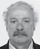
90 nm VLSI interconnects (Source TSMC)
Reproduced by permission of IBM
Let’s take a look at some prominent examples to better understand the definition categories of Marvels of Microelectronic Engineering. The senior EDS members will certainly remember that metal interconnects in the 70’s were based on aluminum not on copper as today. Aluminum, in fact, is even easier to handle than copper, since it can be dry-etched to shape interconnect lines and is less of a headache than copper which might act as a mid-bandgap trap in silicon and, thus, would dramatically increase leakage currents at device junctions unless precautions, such as diffusions barriers, are employed. However, right after Bob Noyce at Fairchild proposed the planar wafer integration process in 1959, it became obvious that such narrow and thin metal lines would be prone to electromigration, an electrochemical material transport that would lead to an interruption of powered metal lines. This was a particularly nasty problem because it could show up on the customer’s side when using the chip. The solution to this problem is an exemplary case of a coincidental discovery with an enormous impact. Without this Marvel Moore’s Law might not even have taken off the ground.
It was in the late 1960’s that IBM researcher Francois d’Heurle was asked to look into this bottleneck issue. In his lab he did experiments with several kinds of metals which he deposited in his electron-beam evaporation system. The aluminum lines that were formed out of his ‘aluminum’ turned out to be far more resistant to electromigration than the Al interconnects of the product technology at that time. Even though this was good news, nobody could make sense of it until Francois found out that the electron-beam also hit the cold copper crucible next to the aluminum. It was then a logical step to intentionally incorporate a small fraction of Cu into Al, thus introducing the AlCu interconnects that are still used today for certain products. This was even the foundation of the Cu interconnects which became inevitable as AlCu hit the electromigration limit in the 1980’s. Francois d’Heurle filed a patent on his Marvel in 1969 and received the IEEE Cledo Brunetti Award in 1988 for this breakthrough discovery by him and his colleagues. This was emblematically the beginning of the “contamination aware” era in microelectronics: electrical engineers needed to watch at the purity and possible doping/alloying of the materials or chemicals they were using to obtain good yields and ensure reliability. Microelectronics was no more an electronic engineers business but became a cross disciplinary research field between electronic, materials and device scientists.
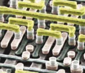
The first CCD prototype by George Smith and colleagues at Bell Labs in 1970 (Reprinted with
permission from George E. Smith, “The Invention and early history of the CCD,” J. of Applied
Physics, May 31, 2011. Copyright 2011)
Another class of Marvel relates to the charge-coupled device (CCD) invented in 1969 at Bell Labs by Nobel laureates William Boyle and George Smith who is an EDS Celebrated Member. The CCD was first intended as a shift register since the focus of the group was on bubble memory. Just one year after its invention Smith and his colleagues could show that the CCD could as well be used as an electronic imaging device. The EDS web site reports: ‘The device they initially sketched was an image sensor based on Einstein’s photoelectric effect, in which arrays of photocells emit electrons in amounts proportional to the intensity of incoming light. The electron content of each photocell could then be read out, transforming an optical image into a digital one. The charge-coupled device they created gave rise to the first CCD-based video cameras, which appeared in the early 1970s. “It took about an hour and half to design the CCD,” joked George, “but it took 40 years for us to get the Nobel.”’ The CCD clearly is a case of an underestimated application, first intended and engineered for a particular purpose but then carried over to an entirely unexpected application. Even though CMOS active pixel sensors have a considerable market share of electronic imagers, even today, after more than 40 years the CCD imager concept drives an ever growing industry.
The third class of Marvels relates to the underrated impact of a discovery which may even have been considered useless, as EDS Celebrated Member Simon Sze quoted his former boss at Bell Labs. Simon Sze and Dawon Kahng came up with the concept and first experimental results of a floating-gate MOS device in April 1967. They called it Floating-Gate Memory (FGM) and wanted to publish it in the IEEE Transactions on Electron Devices but only got permission for a paper in the Bell System Technical Journal where it appeared in July 1967. Their FGM device had a second metal gate for the charge storage. Coincidentally, other teams were exercising their curiosity on the capability to store charges inside the gate insulator of the first p channel IGFETs (Insulated Gate Field Effect Transistor). Following a preliminary idea of Szedon at 1967 DRC on alterable MNOS structures, H.A.R. Wegener from Sperry Rand Research Center published a similar structure at IEDM 1967, in which charges were stored in silicon nitride layer traps by injection through the underlying tunnel native oxide, resulting in a memory device with low charge retention capabilities (a few months at room temperature), due to the leakage with the gate or channel. During the same exploratory period, the use of an extra oxide layer on top of silicon nitride was proposed to implement MONOS structures (Keshavan and Lin from Westinghouse at IEDM 1968, and Keshavan’s patent 1968), introducing one more degree of freedom to bandgap engineering and applied voltages to write or erase the memory element. Programming (erasing) voltages were in the range of -40 to -50 V (+ 40 to +50 V). Still data retention, endurance and scalability of these devices were major issues. In 1977, almost 10 years later, P.C.Y. Chen published a n+ polysilicon gate SONOS device which partially solved the retention time issue of Szeldon-Wegener’s MNOS by oxidizing the nitride layer at high temperature and relaxing the channel tunnel oxide thickness from 15 to 30 Angstroms, reducing the programming voltages to about 20 V, reducing at the same time, but not suppressing, the gap of co-integration with low voltage logic MOSFETs. A huge zoo of possible candidates inhabited the literature. Even though Chen opened a new opportunity, scaling these devices inside a memory array was a major hurdle because the tunnel oxide thickness was already at its limits and endurance (write/erase cycles) would not be meeting large public applications requirements. At that time, the usage was limited to code and not applicable for massive data files storage. UV erasable and hot electron programmable EPROMs had by far the highest density, using the floating gate to store charge and the ONO layer as a coupling capacitor between the control gate and channel. Whether one-time programmable or multiple times programmable devices would be needed depended much on the application. Fujio Masuoka and his team at Toshiba faced the challenge to make collective erasing of memory sectors by a common erase gate while keeping a NOR type structure for individual cell programming. They named the new architecture Flash EEPROM (1984). Further on, a serial arrangement of bit cells into a NAND type structure was proposed (1987) by the same team. The quest for a solid state disk based on transistors was possible by using a NAND Flash scheme, thus reaching more than several 106 write/erase cycles, 10 years retention times and high density (less than 5F2 transistor feature size in an array string) were mandatory. The compromise between reliability and speed would depend on the physical process used for write and erasing. Fowler-Nordheim injection was suited for high capacity NAND Flash (preferably Stand Alone) while low capacity NOR type would still be bearing hot electron programming (preferably Embedded). Under these particularly stressful conditions, combining the difficulties to use high write/erase voltages and increasing the memory density posed very particular problems in scaling and ensuring device reliability.
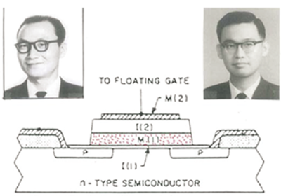
First floating-gate memory (FGM) by Dawon Khang (left) and Simon Sze (right).
(Courtesy of Simon Sze)
Many companies worldwide (Toshiba, Samsung, Hynix, STMicroelectronics, Macronix, Micron, Hitachi, Matsushita,…) have carried out huge struggles in the 1990’s and 2000’s to scale down the ONO stack and the tunnel gate oxide, make sure that short channel devices electrostatic integrity and low parasitics between adjacent cells were kept. A major limitation to the tunnel oxide scaling came from stress induced leakage current (SILC), leading to retention and endurance degradation. This limit reintroduced the interest in barrier engineering based on a revised SONOS concept discrete trap storage. Actually, a TANOS (TaN/Al2O3/Si3N4/SiO2) with a p+ control gate, Macronix 2005) was used to obtain good data retention. Increasing capacity without dimensional scaling was necessary because of the tunnel oxide scaling limitation. 3D integration (Toshiba BICS 2007) was proposed and could include multilevel programming as well.
Today’s flash-memory transistors are close to Kahng’s and Sze’s FGM device with the differences at the levels of physical structure and operation modes. The operation mode of NAND Flash memory is counter intuitive as compared to the initial FGM, because of its collective program/erase operation and serial reading mode, just as in a CCD. Trying to sort out if the credit for the most significant and pioneering contribution to flash memory would go to Kahng/Sze, Wegener, Szedon, Keshavan/Lin,Chen and Masuoka seems not worth discussing. Without the early work of Kahng/Sze and Wegener in 1967, Szedon in 1967, and Keshavan/Lin in 1968, the concept of charge-storage memory may have been considered much later and not in time for conquering its present significance. Without the work of Chen in 1977 and Masuoka in the 1980s that concept may not have made it into practical use and EEPROM may not have taken off the ground or at least much later. Without EEPROM and its short comings when scaling down and operating the device Masuoka’s flash memory may not be there where it is today. The story of flash memory is, thus, not based on a solitary marvel but rather a marvelous chain of discoveries and outstanding engineering efforts in the course of almost 20 years.
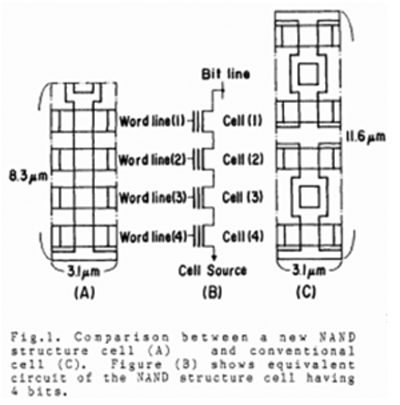
First paper on NAND Flash Memory by Masuoka et al. IEDM 1987
As we already mentioned, the phenomenon of seeking grails is not limited to microelectronics. In the area of photonics, the invention of the blue LED is also emblematic whereas it made white lighting possible and up-scalable. The realization of the first room temperature blue emitting InGaN (Nakamura 1992) was a determinant step to further complete the set of red and green LEDs that would make white lighting possible. Initially, EDS Celebrated Member Herbert Kroemer introduced in 1963 the double heterostructure (DH) based on high-bandgap/low-bandgap materials to realize high efficiency lasers and LEDs. There were many hurdles to be overcome for realizing cheap and reliable, highly performant GaN/InGaN (DH). First, the GaN epitaxial growth by MOCVD on a sapphire requested high crystalline quality (Akasaki and Amano 1985), and uniformity (Nakamura, Two flow mode MOCVD 1991). A final interstitial H+ de-passivation of holes was necessary to obtain highly conductive p+Mg doped GaN anode (Nakamura 1992, Akasaki and Amano 1989).
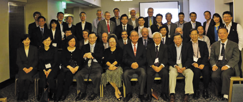
Group photo at the celebration of Prof. Simon Sze’s (mid-front) election to EDS Celebrated Member during IEDM 2017
Finally, a demonstration of a bright Blue InGaN/GaN DH emitting 1 candela was obtained in 1994 (Nakamura). The Indium content allowed tuning the LED color emission from yellow to blue. Commercialization by Nichia Corp. of white lighting devices based on InGaN/GaN LED DHs began in 1996. White lighting based on LEDs is massively used today and has revolutionized lighting thanks to its efficiency and device lifetime: 40% of world electricity consumption would be saved by 2030. The inventions brought by Nakamura, Akasaki and Amano thanks to their flexible up and down scalability, make accessible new lighting modes for mobile phones and large area home displays, automotive, agriculture, healthcare, etc…with the possibility to invent new lighting devices and shapes. The innovation in white lighting by LED represents a major benchmark event of the end of the 20th century history.
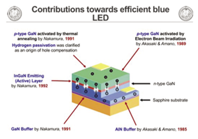
Blue LED history in Nakamura’s Nobel lecture (2014) (Courtesy of S.Nakamura)
The coincidental discovery of AlCu interconnects, the alternate application of the CCD as a solid-state imager, the unforeseen emergence of the flash memory and the invention of blue LEDs are just four examples of Marvels of Microelectronic Engineering. We will search through candidate topics in electronic materials, process technologies, device structures, techniques and semiconductor technologies and try to identify the marvels in those areas as well as their impact on the field.
- October 2018—Electronic Materials—Editor: Simon Deleonibus
- January 2019—Process Technology—Editor: Joachim Burghartz
- April 2019—Device Structures—Editor: Simon Deleonibus
- July 2019—Concepts & Techniques: Editor: Joachim Burghartz
- October 2019—Technologies—Editor: Simon Deleonibus
Your Comments Solicited
Your comments are most welcome. Please write directly to the
Editor-in-Chief of the Newsletter at
clilley@uic.edu