Marvels in Materials Thin Films—Breakthroughs Thanks to Heterostructures
Simon Deleonibus, Past Chief Scientist CEA-LETI |
What is the commonality between SiGe, InGaN and inorganic or organic TFTs, besides the fact that they are based on semiconductors? In all cases, when used as thin film, they are superior and have remarkable properties which can qualify them as marvels of the Electronics and Microelectronics. Heterostructures are the microelectronic fuel to generate electrical amplification and light emission or absorption. SiGe, InGaN and TFTs, have demonstrated their extraordinary power because we can build heterostructures that evidence and value the exceptional properties that thin films can effect on their environment. |
Many years or decades of struggles have been necessary worldwide to come out with commercial applications of high societal impact. In this issue, we illustrate, by three examples, how innovation in materials science and technology had an extraordinary impact on microelectronics advancement. Today’s mobile smart phones are a good example of the combination of integrated multifunctions including the RF Front end, backside lighting and display technology in a single device, which occupies our daily life and is made possible thanks to the science and technology advancements using thin film materials, in little over a century. Thin film heterostructures’ beauty resides as well in the powerful capability to pervade and extend the technology in other domains such as sensors, Si CMOS transistor chip performance enhancement, and public lighting.
The author of this article asked the pioneers in some selected domains to talk about their experience on the way these materials and their process came into play and produced marvels that we find commonly today as being part of our daily life. Joachim Burghartz of IMS CHIPS in Stuttgart in Germany, Shuji Nakamura of UC Santa Barbara in the US, and Arokia Nathan, of University of Cambridge in the UK, accepted to share their experience. Their constructive and knowledgeable cooperation is particularly acknowledged.
SiGe Heterostructures
Heterostructures have often been mentioned in the case of superlattices based on III-V compounds (see hereafter in the InGaN Double Heterostructure section). They can effect in introducing potential barriers, increase electric fields or modify the band structure of the surrounding materials. Pioneering work on SiGe/Si superlattices growth started by Kasper (Applied Physics 1975) at AEG and John Bean’s team (Applied Physics Letters, jan. 1984) at Bell Labs, both with Molecular Beam Epitaxy (MBE). They demonstrated the feasibility of Si1-x Gex pseudomorphic epitaxial growth. Following these premiminary studies, exploratory research on SiGe limited reaction processing started in Jim Plummer’s group at Stanford. This effort moved to IBM, thanks to the former Stanford PhD graduates Hans Stork, Gary Patton, David Harame and Emmanuel Crabbé. Initially, they wished to realize an idea proposed by Herbert Kroemer in 1954 on the benefit on the base transit time from establishing a drift region between the emitter and the collector through the base region by a graded bandgap junction. By that time, Kroemer already had mentioned a SiGe alloy as a possible solution.
The first publications reporting working SiGe bipolar transistors that were superior in performance when compared to their Si counterparts appeared in 1988 from IBM (Patton et al) and 1989 from Stanford (King et al) (Figure 1) both in EDL, reporting on two radically different base materials featuring 12% and 31% Ge, 1000 Å and 1300 Å thick, respectively. In the first case at IBM, the collector, the strained base and emitter were obtained by Molecular Beam Epitaxy, whereas the Stanford team, in the second case, used the limited reaction processing mentioned, a rapid thermal CVD technique. Band offsets between the SiGe alloy base and collector/emitter were clearly observed, reporting increased current gains and Early voltages but still remaining unexplained interface defects and possible SiGe film instability. In the late 1980’s, IBM was looking for a fundamental technology improvement of their implanted-base double-poly self-aligned transistor technology, which was limited in base width and transit frequency. At that time I was a PostDoc at IBM,” says Joachim Burghartz. “We were able to demonstrate the first selective epi base transistor, which was published in EDL in 1988, but gave up on any further effort due to several technical difficulties we encountered, particularly loading effects of the selective epitaxy process and resistance by IBM’s product division to apply selective epi in manufacturing. Ironically, the selective epi base idea for SiGe bipolar was picked up by NEC and Hitachi in Japan.” First results were based on selective MBE and were published at IEDM 1990 by Fumihiko Sato et al. from NEC. Hatsuya Oda from Hitachi showed 130 GHz SiGe selective epi base transistors at IEDM 1997.
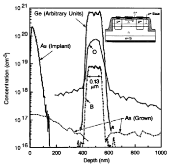
Fig.1. SIMS vertical profile of SiGe HBT. The SiGe film contained 31% Ge (Stanford University IEEE Electron Device Letters, Feb 1989)
All together, three SiGe epitaxial growth techniques and three self-aligned SiGe bipolar transistor technologies were investigated at IBM at the same time. Bernie Meyerson used UHV/CVD epitaxy at temperatures as low as 500°C. Subu Iyer used on MBE and Tom Sedwick worked on APCVD. Achieving high performance SiGe base HBT competing with established bipolar devices met several major technical hurdles to make it manufacturable and cost effective. Struggles had to be faced with SiGe film stability compatible with short base transit time, sufficiently high Gummel number, minimum parasitics and, through modest Ge content, maintaining the instrinsic SiGe base strain during high temperature dopant activation anneals and preventing from dopant outdiffusion from the intrinsic base. A double self-aligned polysilicon architecture responded to the first two requirements.
“Gary Patton and colleagues (Figure 2) demonstrated a superior SiGe bipolar transistor in a paper in the IEEE Electron Device Letters in April 1990, using a built-in drift field in the base region according to Herbert Kroemer’s old idea of the drift transistor and exploiting Bernie Meyerson’s UHV/CVD epitaxy. At about the same time Erich Kasper’s group at AEG in Germany worked on an implementation of Kroemer’s idea of the wide bandgap emitter, though using MBE which was unlikely transferrable to a manufacturing process. For about a couple of years it was a race for record transit frequencies between IBM’s SiGe drift transistor concept and AEG’s SiGe HBT.“, proceeds Burghartz. However, these structures were not self-aligned. “At IEDM in 1990 (Figure 3), we demonstrated record circuit performance for SiGe versus Si bipolar devices for a double-poly structure and for a single-poly device, showing ring oscillator delays below 30 ps”
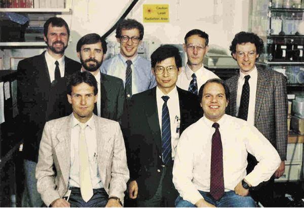
Fig.2. IBM SiGe Team in 1990 showing from left to right side: Joachim Burghartz, Hans Stork, Gary Patton, Jim Comfort, Jack Sun, Edouard de Frésart, David Harame and Emmanuel Crabbé (courtesy J. Burghartz)
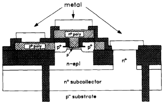
Fig.3. SiGe base double poly HBT by the SEEW (Selective Epitaxial Emitter window) architecture (IBM, IEDM 1990)
The last hurdle was overcome by incorporating Carbon in SiGe: very small amounts (less than 1%) were necessary to limit Boron outdiffusion from the intrinsic base, especially during high temperature anneals or by transient enhanced diffusion. High Carbon content induced a band offsets and compensated SiGe/Si strain from compressive to tensile. The credit for the real breakthrough research on SiGe:C goes to IHP in Frankfurt/Oder (Jörg Osten and co-workers at IEDM 1999) but the first demonstration was achieved by Princeton (Jim Sturm’s team, IEDM 1996).
“Today, the SiGe and SiGe:C epitaxy processes look more like Tom Sedgewicks single-wafer APCVD, the device integration is double-poly self-aligned and the SiGe base profile reflects a trade-off between a heterojunction bipolar device and a drift transistor” concludes Burghartz. Most of the results obtained during the research on SiGe HBT have been transferred to the achievement of BiCMOS architectures, thanks to the growing business of telecommunications requesting low power as well as high frequency capabilities. Basically all BiCMOS technologies on the market today are based on SiGe or SiGe: C. David Harame and B. Meyerson at IBM mainly contributed to its popularity. Not to forget former IBMer John Cressler, now at Georgia Tech and previously at Auburn University, who educated numerous students who are keeping the SiGe technology advancement and industrial application going.”
SiGe today is also used to locally strain bulk pMOS channels (Intel at IEDM 2004) by epitaxial growth in the source/drain areas. It is also applied to add uniaxial strain to already biaxially strained ultra thin body n(Si) and p(Si0.7 Ge0.3)-channel SOI transistors, thanks to respectively SiGe:C and SiGe elevated sources and drains (LETI at VLSI Technology Symposium 2005; LETI, STMicro, IBM at IEDM 2013). The multilayered SiGe/Si, featuring SiGe layers thinner than a critical thickness depending on Ge content, allows to build up to 19 multiple defect free stacked Gate all Around Si Nanowires channels (LETI, STMIcro at IEDM 2006), delivering MOSFETs record saturation current per footprint. The work achieved on Si/SiGe heterostructures since the 1980s is for sure the foundation of the extension to modern CMOS technology.
InGaN Double Heterostructures for Blue LEDs and White Lighting
As we already mentioned, the phenomenon of seeking Graals is not limited to microelectronics. In the area of photonics, the invention of the blue LED is also emblematic whereas it made white lighting possible and up-scalable. The realization of the first room temperature blue emitting InGaN (Nakamura 1992) was a determinant step to further complete the set of red and green LEDs that would make white lighting possible. In this field, Herbert Kroemer left his marks as he proposed the SiGe base/Si heterostructures drift region to improve HBT performance (1954), already mentioned hereabove in the SiGe section. Later, Kroemer (1963) introduced the double heterostructure (DH) based on high band gap/low band gap materials to realize high efficiency lasers and LEDs (Figure 3a). There were many hurdles to be overcome to realize cheap and reliable, highly performant GaN/InGaN (DH). First, the GaN epitaxial growth by MOCVD on a sapphire requested high crystalline quality (Akasaki and Amano 1985), and further crystal improvments (Nakamura, Two flow mode MOCVD 1991).
Professor Shuji Nakamura, 2014 Nobel Prize in Physics, kindly accepted to give us some details concerning his research: “In 1989, I started GaN growth after getting a commercially available MOCVD, after coming back to Japan from USA. I tried to grow GaN epitaxial films on sapphire substrates for a couple of months. However, I mostly did not observe GaN deposition, or even if there was growth, the color of the GaN film was black. Then, I started to modify the MOCVD system every morning by cutting and welding the quartz, graphite, and other materials of the reactor. Every afternoon, I ran the epitaxial growth of GaN at least 3–5 times to check the new modifications by changing the growth conditions. I continued in this manner every day for one-and-a-half years. In October 1990, I completed a totally new MOCVD reactor, named the two-flow (TF) MOCVD. Conventional MOCVD had one horizontal flow to achieve a laminar flow. I added another vertical flow to suppress the thermal convection caused by the high temperature and atmospheric pressure growth. When I grew undoped GaN using the TF-MOCVD, the residual electron mobility was the highest ever reported. In my life, I never experienced a world record. This was my first experience. Since the invention of the TF-MOCVD, and owing to the system’s performance, I was able to achieve breakthroughs in the growth of GaN, p-type GaN, InGaN, blue LEDs, and blue laser diodes every 2–3 months.”
Yet, several key breakthroughs were still needed to improve the TF-MOCVD technique to make LEDs working efficiently. A final interstitial H+ depassivation of holes was necessary to obtain highly conductive Mg doped p-type GaN (Nakamura 1992, Akasaki and Amano 1989).
Nakamura reports: “In 1991, I obtained p-type GaN films by thermal annealing for the first time, and I could finally clarify the mechanism of Hydrogen passivation as a hole compensation. Since the beginning of GaN research in the 1960s, this hydrogen passivation of the Mg acceptors had prevented many researchers from obtaining p-type GaN films.
In 1992, I also grew the first InGaN single crystal layers which showed the first band to band blue emission in PL and EL at room temperature. These InGaN layers have been used as emitting layers in all of the blue/green/white LEDs and all of the violet/blue/green semiconductor lasers. Without this invention of InGaN layers, there would have been no blue/green/white LEDs and no violet/blue/green semiconductor laser diodes.”
There has never been any collaboration with the two other 2014 Nobel prize co-recipients Professors Akasaki and Amano of Nagoya University. “Their contribution was: 1) the development of AlN buffer layer to improve the crystal quality of GaN in 1986. 2) the demonstration of the first p-type GaN using electron beam irradiation. However, they could not understand why they got p-type GaN. See figures 3b and c.
Finally, a demonstration of a bright Blue InGaN/GaN DH emitting 1 candela was obtained in 1994(Nakamura). The Indium content allowed to tune the LED colour emission from yellow to blue. Commercialization by Nichia Corp. of white lighting devices based on InGaN/GaN LED DHs began in 1996.
Nakamura’s way to success was atypical and paved with quite a few technical and professional difficulties! From 1979 to 1985, Nakamura worked for Nichia Chemical Ind. to develop GaP and GaAs bulk crystal as a source material for conventional infrared and red LEDs. The sales of those products were poor due to tough competition with big semiconductor and LED companies. His curiosity from the reading of literature was far the strongest to pursue the idea of developping blue LED: he biggest problems in LEDs came from the absence of efficient blue and green devices. If efficient blue and green LEDs were available, there would be a huge market for LEDs. So, I gradually wanted to develop the blue LED myself”. He was lucky to get his company president to provide him a funding to continue his research, went abroad to the University of Florida, one year from 1988, as a visiting researcher to study GaAs on Si using MOCVD, while his boss rejected his funding request to work on blue LED! “One year later, in 1989, I came back to Japan to start the blue LED research. At that time, my dream became getting a Ph.D. degree instead of developing blue LEDs. I never expected that I could invent the blue LEDs myself!”
The inventions brought by Nakamura, Akasaki and Amano thanks to their flexible up and down scalability, make accessible since the beginning of mass production in 1993, new lighting modes for mobile phones and large area home displays, automotive, agriculture, healthcare, etc… with the possibility to invent new lighting devices shapes.
Nakamura asserts on the huge revolution started in the lighting area: “The application with the greatest impact to the world’s energy consumption is that of general illumination, recognizing that one quarter of all the world’s electricity is used for lighting. LED Light bulbs are more than ten times efficient than incandescent bulbs, and they last for 50 years! At their current adoption rates, by 2020 LEDs can reduce the world’s need for electricity by the equivalent of nearly 60 nuclear power plants. LEDs are also efficient enough to be driven by a simple solar cell powered battery. Now this clean and inexpensive technology can help bring light to millions of people around the world who don’t have access to electricity. LED Lighting has now truly become a reality. Nowadays we can buy energy efficient LED Light bulbs at the supermarket and help reduce energy use. I hope that everyone can use efficient LED Lighting to save energy and do their part to reduce Global Warming.”
White lighting based on LEDs is massively used today and has revolutionized lighting thanks to its efficiency and device lifetime: 40% of world electricity consumption would be saved by 2030. Nowadays, LED manufacturers are trying to optimize the power efficiency and necessary trade off with reliability of the devices. “To maintain high light output, manufactures may use multiple LEDs in parallel, effectively increasing the overall active area and hence reducing current density. The primary origin of efficiency droop is Auger recombination or carrier overflow process.”
“An alternative method to produce white light is by using a blue laser, as opposed to an LED, in combination with a phosphor. Above the lasing threshold, the carrier density is clamped at threshold, fixing its density. Increases in carrier density beyond the threshold density immediately contribute to stimulated emission, or lasing. Thus, the carrier density is maintained at the lower, threshold density, prohibiting it from reaching densities where the Auger recombination process becomes the dominant recombination process. Auger recombination, with the resulting efficiency droop, does not appreciably occur in blue laser diodes.
Current commercial blue lasers have already demonstrated comparable external quantum efficiencies to those of blue LEDs at significantly higher current densities, and hence light output. It is therefore of great interest to further pursue lasers as they have the potential of operating at high current densities, resulting in white light sources with staggering light output.
While laser based lighting has the potential of being more efficient with smaller chip sizes with a very high current density region, it also offers intrinsic directionality of the light output as an ultimate point light source—a feature that car manufacturers have already leveraged in their high-end vehicles …for their headlamps, allowing drivers to see further down the road without blinding oncoming traffic. Future modifications to the laser based lighting technology may well enable the next generation of white lighting with higher efficiencies at lower cost.”
The innovations in white lighting by LED represent a major benchmark event of the end of the 20th century history. The adventure is starting and will continue as long as imagination can permit!
Between a SiH TFT and OTFT
Displays certainly have a very long history dotted with so many disruptions.
Coming up with a low cost solution, capable of meeting high vision quality requirements, together with High mechanical durability and robustness, weight and low power consumption, has been a great challenge since the invention of television. The implementation of transistors and light emitting devices both made on thin films, inorganic or organic, have brought new opportunities such as the volume reduction from 3D to 2D and back to 3D, with different perspectives (!), in many new situations and purposes. The display has become ubiquitous in all areas in our daily life as consumers or professionals have been invested by displays. They are multiformed and must adapt to different substrates: from stainless steel to glass or paper, plastic foils and organic substrates, and many kind of fabrics such as clothing! Today all displays are the active-matrix type, whereas the simple cross point interconnect system(or the passive matrix) of the beginning was a serious hurdle for mastering their power consumption and poor resolution. Concommittently, Thin Film Transistors (TFTs), have followed MOSFET history since the beginning of their developments. Nevertheless and ironically, the challenge of large area electronics with the hybrid integration of the vision grid, produced at low cost, was specific to the world of displays. It was the price to pay to win the struggle of entering into the consumer electronics business.
The ancestor of TFT was described by it’s function as an Insulated Gate Field Effect Transistor (IGFET). The device imagined by the Dundee University team were considered as laboratory characterization tools for materials development purposes (Figure 4a).
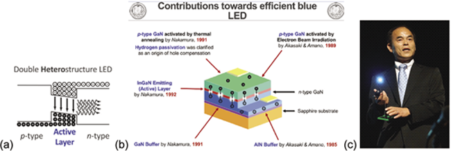
Fig.4. LED principles and history. (a) Double Heterostructure band diagram and light emission process; (b) Blue LED history in Nakamura’s 2014 Nobel lecture; (c) Shuji Nakamura showing a blue LED during his Nobel lecture (all figures by courtesy of S. Nakamura)
In the late 1960s and 1970s, the research on amorphous semiconductors and more specifically amorphous silicon(a-Si) were very active worldwide under the seminal impulses of N.F. Mott (University of Cambridge, UK), 1977 Nobel Prize. Arokia Nathan comments: “Prior to the disclosure of the TFT, display panels (based on twisted nematic mode liquid crystal sandwiched between polarisers) were addressed by a matrix of row and column (X-Y) interconnecting lines. These were referred to as passive matrix displays. T.P. Brody; J.A. Asars; G.D. Dixon had reported a display based on active matrix but using CdSe devices in 1973 in IEEE Trans-ED. But the material led to large charge leakage in the off-state of the transistor serving to undermine display quality. Here the TFT is placed at the junction of the X-Y matrix which when addressed or switched on will rotate the plane of polarization of the liquid crystal thereby modulating the light transmitted through the liquid crystal. The a-Si TFT had far better long-term stability than the II-VI counterpart compounds“. The hydrogenation of glow discharge deposited, so-called today: Plasma Enhanced Chemical Vapor Deposition(PECVD), a-Si brought in by the Dundee team was for sure a major roadblock to overcome before the association of TFT and Liquid Crystals to make large area and reliable flat displays(LCD) in the early 1980s. The drastic passivation and reduction of defects made n and p (type doping of a-SiH possible and drastically increased the mobility in the material. Prior to this was the discovery of the “liquid crystalline nature of cholesterol” in 1888 by Friedrich Reinitzer and further works of Otto Lehmann (1904) on Liquid Crystals and Charles Maugin (1911), who experimented the first “liquid crystal confinement” in betwen two electrodes! Commercial devices became available not before the 1960s Nathan says: “Between 1964 and 1968, at the RCA David Sarnoff Research Center in Princeton, New Jersey, George Heilmeier with Louis Zanoni and Lucian Barton, devised a method for electronic control of light reflected from liquid crystals and demonstrated the first liquid crystal display. This was the passive matrix display.”
Looking back to the past makes us appreciate even more the many breakthroughs this field has gone through, in a 50 years time frame. That is especially due to the wide range of applications and also the huge public that is eager to use them in so many different ways.
“New generations of displays have evolved—a good example being the active matrix organic LED display or AMOLED displays (Figure 4b) which come in the form of cell phone displays and TV screens. Other displays include the electrophoretic display which is used in E-books. TFTs have also evolved and they can be made with organic materials making them amenable to printing technologies. This has now led to the emergence of flexible electronics and displays which can be rolled/folded and is expected to soon hit the market. Pushing more into the future, are wearable devices for health care monitoring where power consumption can become a critical issue making ultra-low power operation a must!,” says Nathan.
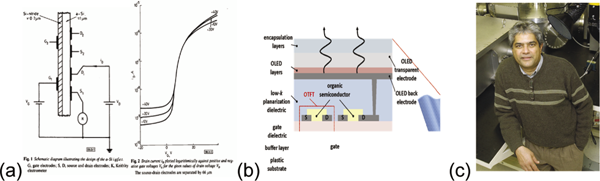
Fig.5. (a) Detail of first publication on amorphous Silicon IGFET, by P.G. Le Comber, W.E. Spear and A. Ghaith in Electronic Letters, February 5, 1979, suggested to address displays active matrix LCDs; (b) AMOLED addressed by OTFTs on flexible substrate; (c) Arokia Nathan (b and c by courtesy of A. Nathan)
Light emission from Organic materials has been investigated since the 1950s (Bernanose et al. J. Chim. Phys., 1953). However, the world›s first working OLED was demonstrated in 1987 by Ching W. Tang and Steven Van Slyke at Eastman Kodak. Active matrix OLEDs have established their huge success thanks to their lower power consumption (a factor of 10 less), higher reliability and application on large surfaces free of form factor. Main display and TV manufacturers such as Samsung, SONY, LG have been very active in the production of high capacity large area displays since the mid years 2000, still relying on the success of TFTs to address the light emitting devices. Today, 65 inches diagonal rollable TVs based on AMOLED technology have been demonstrated (by LG in the January 2018 CES).
OTFTs have now emerged because their low process temperature that matches well for the multiple applications of AMOLEDs on various substrates such as paper, plastic, etc… Although high quality a-SiH could be obtained at these low process temperatures it is form-factor constrained. The discovery of conductive polymers by Shirakawa, Heeger, and MacDiarmid in 1977 was certainly a sign to boost the organic electronics field. They were awarded the Chemistry Nobel Prize in 2000. Significant conductivity/doping results comparable to inorganic semiconductors were obtained in the 1980s and with the achievements of the first organic channel transistors based on polyacetylene/polysiloxane (Ebisawa et al, JAP 1983). Given the wide scope of the applications they might serve, AMOLED and OTFTs already have a huge societal impact. Significant work (see for example Nathan’s team publications in Science, October 2016 and IEEE J. ESTCS March 2017) has been reported to compensate material shortcomings to extend the lifetime of systems based on disordered materials encompassing TFTs and OLEDs.
Your Comments Solicited
Your comments are most welcome. Please write directly to the
Editor-in-Chief of the Newsletter at
clilley@uic.edu
Your Chapter Could Be Missing Important
Notices and Funding Opportunities!
Please remember, whenever there is a change to Chapter Officers, both IEEE and EDS must be notified. Please follow these two steps:
- Report officer changes to IEEE via the vTools Officer Reporting form: https://officers.vtools.ieee.org/ (access to vTools requires use of an IEEE account).
- Report officer changes to EDS by completing the Chapter Chair Update Form: https://ieeeforms.wufoo.com/forms/pgu6n1i1ixepnu/
Thank you in advance for your assistance.