Technical Briefs
A Review of the 2020 IEEE
International Conference
on Microelectronic Test
Structures (ICMTS)
By Stewart Smith, General Chair of ICMTS 2020, University of Edinburgh
Carlo Cagli, Technical Chair of ICMTS 2020, ST Microelectronics
The 33rd International Conference on Microelectronic Test Structures (www.icmts.net) sponsored by the IEEE Electron Devices Society, was due to be held in March 2020 at the University of Edinburgh, Scotland. However, in response to the worldwide travel restrictions resulting from the COVID-19 pandemic, the event was adapted by the local conference committee, with the help of the IEEE Meetings, Conferences and Events (MCE) team and staff at the EDS, to a three-week online virtual experience. This enabled the technical community of designers and users of test structures to come together to discuss recent developments and future directions in the field.
The ICMTS has been active since 1979 when a workshop was held in San Jose, California. At the event, founder member Dr. Martin Buehler, delivered his seminal paper entitled Comprehensive Test Patterns with Modular Test Structures: the 2 by N Probe-Pad Array Approach, which led to the standardization of test structure design and automated parametric test. It was this workshop that grew into the IEEE-supported, peer-reviewed annual conference now in its 33rd year of service to the semiconductor industry, alternating between Europe, the United States, and Asia. Dr. Buehler passed away in 2018. A search of his work uncovers an impressive collection of technical papers, books, and many other documents detailing the best-known methods of device evaluation. Martin brought his technical skill to ICMTS, helping to guarantee the value of this congress, but also energized meetings with his sense of humor and wit, making them both informative and fun events to attend. His spirit lives on with each new edition of the conference, and the ICMTS appreciates his vision and technical acumen. We offer our most sincere condolences to Martin’s family and friends. May he Rest in Peace.
Attendees of the 2020 event were able to experience a full programme of technical papers covering a diverse range of topics in the areas of advanced measurement techniques, parametric test, noise measurement, and the characterization of materials, MEMS processes and devices and a wide range of microelectronic devices including MOSFETs, RF and optoelectronic devices. Unfortunately, the extraordinary circumstances resulted in the cancellation of the popular tutorial session. The tutorial chair, Prof. Francesco Driussi of Università degli Studi di Udine, Italy had prepared a series of exciting and informative lectures that would have taken attendees from a textbook-level of knowledge through to an understanding of the current leading-edge research in test and measurement. These included some of the current hot topics in microelectronics such as 2D materials, advanced packaging and neuromorphic computing. It is hoped that a number of the speakers who were due to give tutorial lectures, will be able to accept the invitations that have been made to present at the 34th edition of the conference in 2021.
Even within a virtual environment, the conference was still able to offer two excellent keynote presentations. The first entitled History and future of measurement instruments for semiconductor parameter analysis was given by Satoshi Habu of Keysight Technologies, Japan. The talk gave a review of the tools of microelectronics measurement from the first source measurement unit (SMU) based instrument introduced in 1982, through to modern day parameter and device analyzers. With his many years of experience, Habu-san was also able to give the audience an insight into expected future trends in measurement instrumentation. The second invited presentation entitled Experimental Set-Up For Novel Energy Efficient Charge-based Resistive RAM (RRAM) Switching was given by Paola Trotti of CEA Leti, France. This work explored an important current trend in non-volatile storage, the resistive random access memory (RRAM). In particular, it detailed a new method to reduce the energy consumption during the writing of process-spread RRAM, based on setting an initial electrical charge into a writing capacitor rather than applying constant voltage over a fixed time. Presented results showed that setting the initial charge is a better choice to efficiently control the variability of the filamentary process in RRAM.
All of the peer-reviewed papers accepted into the technical programme were of a very high standard. A number of noteworthy papers are highlighted here, in particular those that vied for the coveted best paper prize. The winner, decided with a vote by the members of the technical program committee, was a paper presented by Bruna Cardoso Paz, from CEA-Leti based on the MINATEC Campus of the Université Grenoble Alpes, France, entitled Integrated Variability Measurements of 28 nm FDSOI MOSFETs down to 4.2 K for Cryogenic CMOS Applications. The excellent video presentation looked at mismatch performance of 28 nm FDSOI technology MOSFETs operating at very low temperatures. Of keen importance in quantum computing applications, the mismatch of advanced CMOS node transistors operating at cryogenic temperature regimes has not been extensively explored. For the first time, this paper presented a variability study of FDSOI MOSFETs down to temperatures as low as 4.2 K, identifying slight degradation in variability at these liquid helium equivalent temperatures, see figure 1. The understanding gained from this kind of work is essential in the development of accurate compact transistor models for circuit design, and the presentation resulted in an active discussion board exchange.
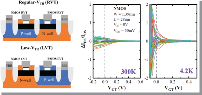
Fig. 1. Schematic of 28 nm FDSOI NMOS and PMOS devices with regular and low threshold voltage designs (left). Drain current variability as a function of the gate voltage overdrive at 300 K and 4.2 K (right).
Another paper that caught the attention of the attendees was given by Hans Tuinhout of NXP Semiconductors in the Netherlands. His latest work on the spatial distribution of mechanical stress in semiconductor devices was presented in a very lively and easy to follow video entitled Characterization of parametric mismatch attributable to plastic chip encapsulation. The work developed a test structure and associated high-precision characterization approach to the measurement of mechanical stress during several stages of the packaging flow. The structure involving more than 2000 individual measurement cells was arranged within an array underneath the wire bonding pads. Data presented in the paper quantified substantial systematic effects caused by lead frame mounting and wire bonding as well as subtle random variability occurrences attributable to the spatial distribution of silica particles in the molding compound, see Figure 2. The paper also considered the addition of a chipcoat gel stress buffer layer prior to encapsulation to mitigate the impact of silica particles. The discussion board Q&A saw a lively exchange regarding the size and position of silica particles, usage area of the test structure array, the wirebond effect before and after adding the chip-coat gel as well as stress relief dependency on chipcoat temperature.
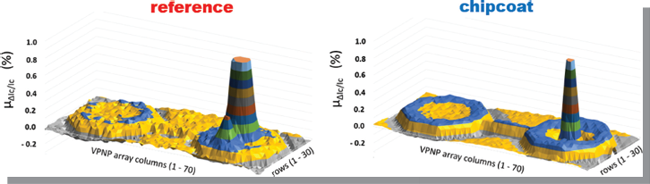
Fig. 2. Collector current variability changes across arrays of 2100 vertical PNP transistors due to packaging in plastic. The raised areas are the aluminum pads and the spikes are caused by bond wires. The noisiness of the reference (left) is attributable to silica particles from the molding material, and is suppressed by applying a chipcoat gel (right).
Test structures developed for the study of microelectromechanical systems (MEMS) design and fabrication have become an increasingly popular subject area at the ICMTS meetings in recent years. In a paper entitled Test structure for measuring etch selectivity in vapour etch processes, Markus Ronde of host organization, the University of Edinburgh detailed the development of a novel test structure and characterization method to study etch selectivities between material layers in a sacrificial release process using an isotropic vapour etch technique. Until now it has proved difficult to simultaneously measure the etch rates of adjacent layers accurately, leading to false assumptions about etch resistance. The developed test structures consist of free-standing bridges that can be deflected by a mechanical surface profilometer to indicate the extent of material removal in a stack of sacrificial and structural layers. This was used to study the etch selectivity between a structural layer of silicon nitride and a polysilicon sacrificial layer when using a XeF2 vapour etch process. The results demonstrated that the silicon nitride is etched at an enhanced rate when it is located in the proximity of the sacrificial polysilicon layer being removed, which goes against previous claims that the layers are largely inert when exposed to the vapour etchant. This represents an important result for the development of devices incorporating freestanding structures.
In the area of noise measurements, a highlight was the paper by Aarthi Jayakumar of Global Foundries, entitled Area-Efficient and Bias-Flexible Inline Monitoring Structure for Fast Characterization of RTN and Transistor Local Mismatch in Advanced Technologies. The presentation detailed an improved set of scribe line monitors with high device densities, which have been designed to enable inline monitoring of random telegraph noise (RTN) and transistor local mismatch. Accurate characterization of these parameters is necessary in order to improve the analog performance of integrated circuits. The structures have been designed with a small footprint to allow placement within narrow scribe lines. They are also flexible enough for usage across different oxide types, threshold voltage ranges, and device geometries. The paper demonstrated the parallel testing capability of the structures, which enables rapid data collection ensuring efficient testing times.
Other highlights include a paper from Gilgueng Hwang of the University of Tokyo entitled A Rapid, Reliable and Less-destructive On-chip Mass Measurement for 3D Composite Material Testing Microstructures. This work demonstrated a rapid, reliable on-chip method of measuring the mass of delicate 3D microstructures through a shift in resonant frequency. The method is based on atomic force microscopy, and has been demonstrated by the characterization of MEMS structures with complex helical geometries. The measurement sensitivity is revealed to be 25 Hz/pg and shows great promise for testing of both 2D and 3D structures as well as composite materials. Also of note was the paper from Brad Smith of NXP Semiconductors in Austin, Texas entitled Calibration of CBCM Measurement Hardware, which described a test structure designed to enable validation of a test hardware’s limits prior to its use in AC circuit design. The test structure can mimic a charge-based capacitance measurement by delivery of periodic spikes of current of three magnitudes and at a wide range of frequencies, created by a series of inverters. Current measurements using a commercially available parametric tester were shown to be completely linear with frequency across a four-decade frequency range, and for average currents as low as 530 pA, see Figure 3.
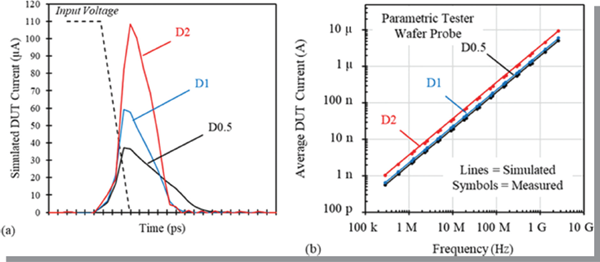
Fig. 3. (a) Simulated device under test (DUT) currents for three inverter drive strengths when the input voltage drops from high to low. (b) Measured and simulated average DUT currents for 24 frequencies per inverter drive strength, measured in wafer form on a parametric tester.
The ICMTS virtual event included an Exhibitors Area, which allowed attendees to view videos and download content that highlighted the latest commercial advances in measurement and test equipment solutions. This year’s event was sponsored by exhibitors, MPI Corporation, Keysight Technologies, Celadon Systems Inc., ProPlus Design Solutions Inc. and Lambda Photometrics Ltd., as well as by the School of Engineering at the University of Edinburgh. The ICMTS will always be indebted to our sponsors for their unwavering support during the difficult times of 2020.
The technical chair for ICMTS 2020, Dr. Carlo Cagli of ST Microelectronics echoed the thoughts of the whole technical committee in his closing comments. “It has been a challenge, but also an honor, to be involved in the organization of this year’s event. The programme provided by the ICMTS was extraordinarily rich and of high quality, spanned exciting work in diverse fields from MEMS characterization to FinFET noise measurements, through to cryogenic MOSFET characterization and memory test cells. I would like to thank all the authors who contributed to the success of this edition of ICMTS as well as all the members of the technical and steering committees who assured the high quality of the technical program”.
It is a remarkably interesting aspect of semiconductor evaluation that the manufacturing process takes about 60 to 75 days to build a complete semiconductor device. It takes almost that long for management to approve the publication of a technical paper describing the novel characterization knowledge gained from that device! It is with these time constraints in mind that we recommend you begin preparing for ICMTS 2021, which is planned to take place in Cleveland, Ohio in the United States this coming April. We hope very much to be able to hold a live conference in 2021, and we invite you all to participate.