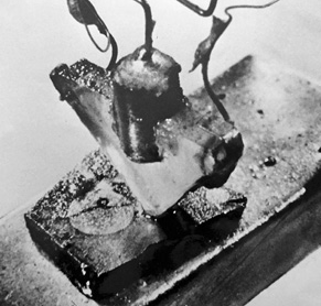
Photo Courtesy: Bell Labs ‘47
|
Photo Courtesy: Bell Labs ‘47 |
The year 1905 is well known as the “Miracle Year” because Albert Einstein published four papers that changed the laws of physics and were significant contributions to the foundation of modern physics. Similarly, November 1947–January 1948 were the three magical months that paved the way for modern-day electronics. This was done by three brilliant scientists who were members of the Mervin Kelly’s Solid State Physics Group and Semiconductor Sub-Group at Bell Labs, which were given the challenging task of creating a solid-state semiconductor switch that could replace the vacuum tube. The famous physicists—Walter Brattain and John Bardeen managed to make the first working transistor, now known as the point-contact transistor. The invention was made on December 16, 1947. A week after that, the device was officially demonstrated to Bell Labs executives as a “magnificent Christmas present.” In January 1948, William Shockley demonstrated the junction transistor. All three received The Nobel Prize in Physics (1956) and as per Nobel Prize Committee—“In 1947 John Bardeen and Walter Brattain produced a semiconductor amplifier, which was further developed by William Shockley. The component was named a “transistor”.”
The Electron Devices Society has decided to celebrate the year 2022–2023 as the 75th Anniversary of the Transistor. As the history of this invention and of its consequences is much more involved and interesting, it is imperative that the leading EDS Luminaries share the scientific & technological developments which took place in the last 75 years, with the current generation of researchers. Popularizing talks at Conferences and Mini-Colloquia, Technical Articles in the EDS Newsletter, Webinar Series shall be a part of the various activities undertaken by the “75th Anniversary of the Transistor Adhoc Committee” with an aim to provide technical information and education to enlighten EDS members. This shall be a mark of tribute to the men and women who have contributed to the Transistor Story—Discovery, Development, and Applications which has had a lasting impact on people’s lives and has benefited mankind where it serves good in social relations, caring for the Earth, science, technology, engineering, and economy.
Manoj Saxena
75th Anniversary of the Transistor
Adhoc Committee Chair
75th Anniversary of the Transistor
Invention of the Transistor 75 Years Ago;
The Origin of Device Miniaturization Towards
Super-Intelligent Society
1. Before the Transistor
In the middle of the 19th century, electrical engineering provided us with a big technological leap, i.e., instantaneous long-distance transportation of ‘energy’ and ‘information’ through electric wires. The ‘information transportation’ was conducted at the end of the 1830’s by the electric telegraph with ‘relays’ used as the amplifier of the decaying signal (Morse code) propagating on a long wire [1]. The relay was the first electric device which amplified electric signal, but it had a function of only digital signal amplification by the mechanical switch controlled by the signal current flowing in the electromagnet coil.
Then, 60 years later, wireless telecommunication started with a strong demand for the analog signal amplification. The analog signal amplification was realized by the invention of the ‘triode vacuum tube’ in 1906 [2]. The electron current in a vacuum tube between the cathode and anode was directly modulated by the potential of the ‘grid electrode’ inserted in the electron current flow. The analog signal imposed on the grid bias was transferred into the electron current and amplified. The grid bias can also switch on/off the electron current. The triode vacuum tubes had been widely used for telecommunication and machine control since then. This was the beginning of ‘electronics’ that enabled the manipulation of electron movement in the devices for many applications.
2. The Road to the Transistor
However, the vacuum tubes were not suitable for low power-consumption operation and also for very high-frequency operation at microwave range due to the difficulty of the size reduction. It would be quite natural to imagine that replacing the vacuum tubes by solid-state amplifiers could solve the above problems. The idea was to modulate the lateral current in a solid-state material by the vertical electric field applied by the 3rd terminal, i.e., ‘grid’ or ‘gate’. This is the analogy to the triode vacuum tubes and the idea of the ‘Field Effect Transistor (FET), although the term ‘transistor’ did not exist at that time. However, different from the case of electron current in the vacuum, controlling the electron current in solid-state materials by the vertical electric field was not easy because of the high-density charges of electrons and ions existing in the solid-state materials. Thus, it was assumed to be necessary to use an ‘extremely-thin semiconductor film’ as the solid-state material. The first recorded ideas of the FET were filed as patents without any experimental data in 1925 for MESFETs [3] and 1928 for MOSFETs [4]. Although semiconductors had been already used for commercial crystal rectifiers [5]–[7] from the beginning of the 20th century, the physics of semiconductors such as band theory [8] using quantum mechanics was not known at all until the 1930’s. At that time, there were even no concepts of holes and p-n junctions, and the quality of the semiconductor materials was not sufficient at all [9]. Later in 1945–1948, W. Shockley of Bell Telephone Laboratories thought of an idea of MOSFETs [9]–[12] independently from the previous MOSFET ideas. His idea was to modulate the carrier density at the semiconductor surface by the band bending caused by the vertical electric field from the gate electrode. He predicted the amount of the carrier density modulation based on the calculation using the band theory. However, the experimental carrier density modulations on Si, Ge and Cu2O were 3–4 magnitudes of order smaller than those of the theoretical calculations [9]–[12] because of the existence of the fixed electrons trapped at the surface states [13]. (The accumulation layer conduction with the majority carriers of the MOSFET is shown in W. Shockley’s works [10], but the inversion layer conduction with the minority carriers was not recognized by his works [10], [12]. The inversion type of the conduction was found by J. Bardeen in 1947 [14] and the inversion layer conduction used in today’s MOSFETs was clearly described later by L. Brown’s paper [15] published in 1953). W. Shockley’s group continued the research for preventing the trapped surface charge effect, and fortunately, J. Bardeen and W. Brattain found, on December 16, 1947, current amplification phenomena when they put the 2 gold point-contact electrodes (emitter and collector electrodes)—with the separation of 50 μm—directly onto the n-type Ge surface [9]–[11], [16], [17]. The Ge substrate was connected to the base electrode from the backside. The injection of holes from the emitter electrode under the positive bias condition modulated the potential of Ge near the collector electrode and enhanced the electron current between the base and collector electrodes. This was the first solid-state amplifier and named ‘transistor’ as a contraction of ‘trans-resistance’. The amplification mechanism was different from that of FET, and this transistor is later called ‘point-contact bipolar transistor’ because both majority and minority carriers contribute the amplification.
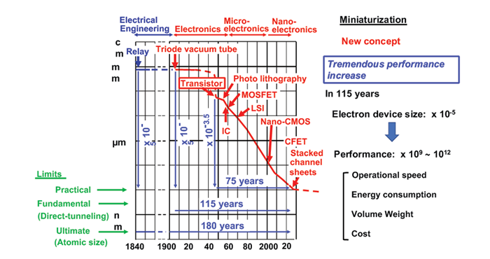
Trend of minimum line width used for devices and performance increase
3. The Transistor as the Origin of the Device Miniaturization and the World After the Transistor Invention
The point-contact bipolar transistor had soon evolved to the junction bipolar transistors (BJT’s) [9], [11], [18] in 1948 in order to prevent the mechanical instability of the contact. Monolithic integrated circuits started using BJT’s in 1958 [19] and 59 [20]. In 1960, the first MOSFET was realized by choosing thermally-grown oxide on Si as the gate oxide [21] in order to significantly decrease the surface trapped charge density. MOSFETs replaced the BJTs in Large Scale Integrated circuits (LSI’s) by the end of 1960’s because of the ease of their integration due to the planar structure.
Now, the minimum line width used for nano-CMOS VLSI is about 15 nm. The minimum line width has decreased about 105 times since the first vacuum triode in the past 115 years, and 103.5 times since the first transistor in the past 75 years, respectively, as shown in the figure. Because of the size decrease, the performance—such as operational speed, energy/power consumption, volume, weight, and cost of electric systems/machines improved billions—trillions of times. The invention of the transistor 75 years ago was the origin of electron device miniaturization, and it was a great technological leap for the progress of intelligent society. Miniaturization of the electron devices towards micro-/nanoelectronics was an extremely important concept. Without the tremendous miniaturization of the transistors in the past 75 years, today’s intelligent society with the internet, and AI would not exist.
4. Future of the Transistor
According to IEEE IRDS (International Roadmap for Devices and Systems) 2021, ‘3 nm’ logic CMOS technology will start production this year (2022), and we can still expect the merit in size, operational-speed and power-consumption. It should be noted that the ‘logic technology names’ such as ‘5 nm’ or ‘3 nm’ are just ‘inflated names’ and have nothing to do with the real physical size used in the devices. Indeed, it is a bad custom of the logic CMOS industry. Real minimum line width such as the gate length is about 15 nm for the ‘3 nm technology’ according to the IRDS 2021. At this moment, the downsizing limit of the minimum line width—such as the gate length and metal wire width—is thought to be about 10 nm because of the significant increase in leakage current of MOSFETs and resistance increase and reliability degradation of interconnects. So, the scheme of device miniaturization, having continued since the invention of the transistor, could reach the limit in several years. Even if we could solve those problems by the introduction of new materials/technologies, it should be noted that 3 nm is the ‘fundamental limit’ caused by the direct-tunneling leakage current, and that 0.3 nm is the ‘ultimate limit’ due to the atomic size. Thus, there will be no ‘pico-technology’ after ‘nano-technology’, and the end of the device miniaturization is not so far.
However, the progress of the integrated circuits with Moore Law will continue by the 3D integration. In IEDM 2020 and 2021, there were many publications of 3D MOSFETs such as CFETs (Stacked nano-sheet channel n- and p-MOSFETs) [22]. The progress of the 3D integration will reach a limit in 10–20 years because of the increasing heat density and cost increase. However, demands for high-performance semiconductor devices with low-power consumption will keep increasing in the future super-intelligent society, and the technology optimization of the devices for each specific application will continue after that. Future intelligent society will create many new business fields such as 6G communication or autonomous driving, which will require new functions and performances. We will have so many things to do for future logic, memory, telecommunication, power, and sensor devices to optimize for the new businesses.
In the long term, the next leap of technology will be the introduction of bio systems. This does not necessarily mean to introduce the algorism of the bio system on semiconductor devices, but also means to use existing bio systems, and the cooperation between the electronics and bio systems becomes important. Even though the champion player of the ‘Go’ game cannot win the AI player because the human brain cannot keep concentration only for one thing for long hours without rest and cannot memorize and remember huge volume of data accurately, bio systems such as brains composed by neurons are much efficient than the semiconductor AI system in most of the cases.
Dr. Hiroshi Iwai is a semiconductor device engineer who contributed to the development of LSI technologies at Toshiba, Tokyo Institute of Technology, and NYCU for almost half a century since 1973. He was the IEEE EDS President (2004–2005) and the IEEE Division I Director (2010–11). He is an IEEE Life Fellow, an IEEE EDS Eminent Lecturer and an IEEE IRDS committee member.
References
[1] S. F. B. Morse, US Patent 1647, filed April 7, 1838.
[2] L. de Forest, US Patent 879,532 filed January 29, 1907.
[3] J. E. Lilienfeld, US Patent 1,745,175, filed October 8, 1926. (Priority October 22, 1925).
[4] J. E. Lilienfeld, US Patent 1,900,018, filed March 28, 1928.
[5] J. C. Bose, US Patent 755,840, Filed September 30, 1901.
[6] H. H. C. Dunwoody, “ U S Patent 837,616, filed March 23, 1906.
[7] G. W. Pickard, US Patent 836,531, filed August 30, 1906.
[8] A. H. Wilson, Proc. Royal Soc. vol. A133, p. 458, 1931.
[9] F. Seitz and N. G. Einspruch, “Electronic Genie: The Tangled History of Silicon,” University of Illinoi Press, 1998.
[10] W. Shockley, IEEE Trans. on ED, vol. 23, p. 597, 1976.
[11] M. Riordan and L. Hoddeson, “Crystal Fire: The Invention of the Transistor and the Birth of the Information Age,” W. W. Norton & Company, 1997.
[12] W. Shockley et al., Phys. Rev., vol. 74. p. 232, 1948.
[13] J. Bardeen, Phys. Rev., vol. 71. p. 717, 1947.
[14] L. Hoddeson, Historical Studies in Physical Sciences, vol.12, p.41, 1981.
[15] L. W. Brown, Phys. Rev., vol. 91. p. 518, 1953.
[16] J. Bardeen et al., Phys. Rev., vol. 74. p. 230, 1948.
[17] J. Bardeen et al., US Patent 2,524,035, filed June 17, 1948.
[18] W. Shockley, US Patent 2,569,347, filed June 26, 1948.
[19] J. S. Kilby, US Patent 3,138,743, filed February 6, 1959.
[20] R. N. Noyce, US Patent 2,981,877, Filed July 30, 1959.
[21] D. Kahng, US Patent 3,102,230, filed May 31, 1960.
[22] L. Liebmann, et al., IEDM, pp. 51, 2021.