75th Anniversary
of the Transistor
Perspectives on Low-voltage Tunnel Transistors for Beyond CMOS Logic
ALAN SEABAUGH
DEPARTMENT OF ELECTRICAL ENGINEERING, UNIVERSITY OF NOTRE DAME,
NOTRE DAME, IN 46556

In this, the 75th year anniversary of the transistor, complementary metal oxide semiconductor field-effect (CMOS) transistors continue to advance, from fin structures to nanosheets and to angstrom technology nodes. In the wake of this development, discussions continue on steep-subthreshold-swing transistors which still hold promise to outperform CMOS at low voltage, but have so far fallen short of the performance needed for applications. It is worth reviewing the development of the tunnel field-effect transistor (TFET) with the aim to stimulate new ideas and fresh consideration of the paths taken and the technical challenges. For a deeper dive, there is a chapter in the just published Springer Handbook of Semiconductor Devices [1] on tunnel field-effect transistors, and there are many recent reviews, search e.g. “TFET review.”
The TFET is an MOS technology and shares many of the structural attributes needed for a transition into a foundry process. A complementary TFET with comparable current drive at lower supply voltage than Si CMOS would enable lower power dissipation without sacrificing speed. The TFET could readily move into the design ecosystem with the primary new device attribute being the steep subthreshold swing. In the MOSFET, the current control mechanism is thermionic emission over an energy barrier, and this sets a fundamental limit on the minimum subthreshold swing at 60 mV/decade change in current at room temperature. The TFET relies on electric field control of tunneling and with this current control, the subthreshold swing can be lower (steeper) than 60 mV/decade.
The n-channel TFET, in planar form, differs from the MOSFET in the polarity of the source-channel junction. In the off state, shown in figure 1 (a), electrons in the valence band of the source are energetically blocked from tunneling into the channel. With a positive gate bias these electrons in the source tunnel into the channel, with current injection set by the overlap of the filled valence band and empty conduction band states in the channel; this is labeled the tunneling window, qVTW, in figure 1 (b). The gate voltage simultaneously modulates both the tunneling probability for injection of electrons into the channel and the availability of empty channel states.
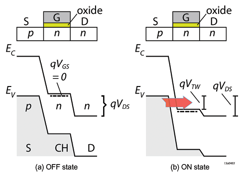
Figure 1. Schematic energy band diagram and cross sections of the tunnel FET.
There is a long history of experimental and theoretical development of tunneling diodes and transistors leading to the TFET [2], [3]. The realization that low subthreshold swing could be achieved by gating of interband tunneling began to appear in publications in 2003 and 2004 [4]–[6]. In 2004, Joerg Appenzeller reported 40 mV/dec subthreshold swing in a carbon nanotube FET explained by interband tunneling [4]. The promise of a transistor that could outperform Si CMOS at low voltages attracted international attention and substantial research investments over almost a dozen years. The list of semiconductor materials and structural embodiments explored experimentally is extensive: Si, Ge, SiGe, III-Vs, III-Ns, 2D materials, mixed heterojunctions, n-TFET, p-TFETs, pillars, nanowires, ribbons, tubes, vertical tunneling, lateral tunneling, and more. A similar breadth of exploration has taken place in theory and design to seed these device developments and interpret the measured device characteristics.
Selected best reported transfer characteristic of the n-TFETs across materials systems are shown in the accompanying figure 2 [1]. These TFETs were selected to show performance at drain voltages less than or equal to 0.5 V (where they would be expected to operate). To be included here the transistors also needed to exhibit subthreshold swing less than 60 mV/dec over at least one order of magnitude in drain current. Across materials systems, it can be seen that the direct-bandgap III-V materials have demonstrated the highest current drives. In comparison with CMOS, the currents are about an order of magnitude lower than desired to outperform Si at similar voltages. Indirect-bandgap materials such as Si and Si/Ge exhibit still smaller currents since phonons are required to enable the tunneling transitions, lowering the tunneling rates. Steep swings in 3D Ge/2D MoS2 and carbon nanotubes are also a part of this comparison.
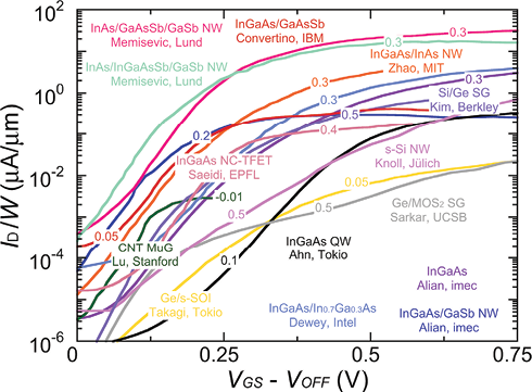
Figure 2. Comparison of selected published n-TFET transfer characteristics. The numbers on the plots are the drain/source voltages. The curves have been shifted to put the current minimum at 0 V. References are given in [1].
The corresponding subthreshold swings as a function of drain current/width is shown in the companion figure 3. One would like the voltage (V60) at which the subthreshold swing becomes less than 60 mV/dec to occur at a drain current of about 1 μA/μm and then to stay below 60 mV/dec for about 4 decades. The current at V60 is denoted I60. The III-V channel materials show an I60 approaching the desired 1 μA/μm, and show steep swing for more than 2 decades. The lower limit on this behavior is attributed to trap-assist tunneling, a leakage mechanism whereby electrons from the source valence-band tunnel into traps in the channel traps (surface or bulk) and then are thermally-emitted to the conduction band. Group-IV-containing materials have generally shown lower leakages and this has led to more extended ranges over which the subthreshold swing stays below 60 mV/decade.
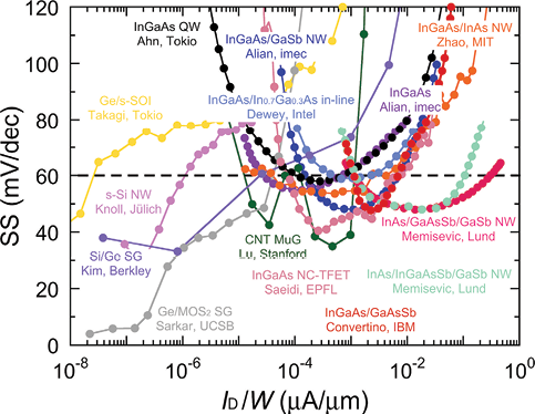
Figure 3. TFET subthreshold swing versus drain current for the n-TFETs shown in figure 2 [1].
While new applications can drive technology development, benchmarks are useful to focus development. For the n-TFET the performance targets which would constitute clear measures of progress relative to the Si n-MOSFET are: drain current exceeding 200 μA/μm at voltages less than or equal to VDS = VGS = 0.4 V, with I60 = 1 μA/μm and maintaining steep subthreshold swing over more than 4 decades. Other measures of progress are the development of a path to a complementary technology and to entry into manufacturing at the leading technology nodes.
To reach these ends will require fundamental studies in materials and devices. Much progress has been made on TFETs, but it is spread widely across semiconductor materials and heterojunctions. Community focus still awaits motivating experimental and theoretical direction. In any particular materials system, how is the abrupt tunnel junction doped, what limits the doping density and abruptness, what is the origin of the band tails, what is the preferred MOS stack and what are the interfacial defects, bulk traps, and border traps? Perhaps there are composite transistor structures that enable TFET operation when the device is operated at low voltages, but enable MOSFET action at high voltages. Perhaps there will be discoveries at the angstrom technology nodes that provide new approaches. Perhaps there are collective mechanisms in complex dielectrics that can be utilized to lower swing without introducing hysteresis. There are many avenues for breakthroughs.
In 1976, approaching the 30-year anniversary of the transistor, William Shockley was asked to write a paper about how the first transistors were conceived and brought to demonstration [2]. A key finding for him in writing this paper was surprisingly “how slow he was and how he missed the junction transistor’s key concepts so many times.” His message to readers facing conceptual and technical challenges was to “stick with it and not give up.” This is clearly a message relevant to TFETs. Experiments show the technical gaps. New solutions are needed to enable manufacturing and commercialization. There are reasons to keep thinking about TFETs.
References
[1] P. Paletti and A. Seabaugh, “Heterojunction tunnel field-effect transistors,” in Springer Handbook of Semiconductor Devices, ed. by M. Rudan, R. Brunetti, and S. Reggiani, 867-903, 2023.
[2] A. C. Seabaugh and Q. Zhang, “Low-voltage tunnel transistors for beyond CMOS logic,” Proc. IEEE, vol. 98, 2095-2110, 2010.
[3] A. M. Ionescu and H. Riel, “Tunnel field-effect transistors as energy-efficient electronic switches,” Nature, vol. 479, 329–337, 2011.
[4] P.-F. Wang, T. Nirschl, D. Schmitt-Landsiedel and W. Hansch, “Simulation of the Esaki-tunneling FET,” Solid-State Electronics, vol. 47, pp. 1187-1192, 2003.
[5] P.-F. Wang, K. Hilsenbeck, T. Nirschl, M. Oswald, C. Stepper, M. Weis, D. Schmitt-Landsiedel and W. Hansch, “Complementary tunneling transistor for low power application,” Solid-State Electronics, vol. 48, 2281-2286, 2004.
[6] K. K. Bhuwalka, J. Schulze and I. Eisele, “Performance enhancement of vertical tunnel field-effect transistor with SiGe in the δp+ layer,” Jap. J. Appl. Phys., vol. 43, 4073-4078, 2004.
[7] J. Appenzeller, Y.-M. Lin, J. Knoch and P. Avouris, “Band-to-band tunneling in carbon nanotube field-effect transistors,” Phys. Rev. Lett., vol. 93, 196805, 2004.
[8] W. Shockley, “The path to the conception of the junction transistor,” IEEE Trans. Electron Devices, vol. 23, 597–620, 1976.
75 Years of Compact Models:
From Shockley to Sticker Shock
COLIN C. MCANDREW, LIFE FELLOW, IEEE AND LAURENCE W. NAGEL, LIFE FELLOW, IEEE
C. C. MCANDREW IS WITH NXP SEMICONDUCTORS, CHANDLER AZ 85224 USA
L. W. NAGEL IS WITH OMEGA ENTERPRISES CONSULTING, KENSINGTON CA 94708 USA
I. Introduction
Today, everyone knows what a “compact” model (a.k.a. a SPICE model [1]) is: an analytical model, hopefully both accurate and computationally efficient, of a (semiconductor) device that is implemented in a circuit simulator and is used for the design of circuits, especially of integrated circuits (ICs).
The archetypical compact model is the Shockley equation for current in a pn-junction diode [2]
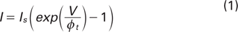
where V is the voltage across the diode, ϕt is the thermal voltage, and IS is the “saturation current,” which can be calculated from physical and structural parameters.
Simplified compact models are also used by professors to teach the basics of how devices work, and by designers to form mental images of how devices work, to help them innovate new circuits.
The size, complexity, and expectations (yield, reliability, performance, power consumption) of ICs have increased exponentially for many years—Moore’s Law—which has led to a concomitant increase in expectations of the capabilities of computer-aided design (CAD) tools, like SPICE, and the compact models in those tools [3], [4].
Here, we give a brief overview of the trajectory of compact models since the invention of the transistor.
Nomenclature: q is the elementary charge, k the Boltzmann constant, T is temperature in Kelvin, ϕt = kT/q, μ is mobility, VAB is the voltage between terminals A and B.
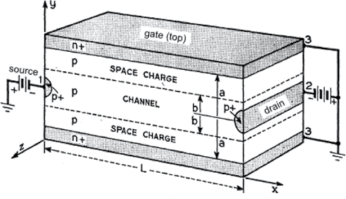
Figure 1. Fig 1 of [5], from 1952, which shows the device abstraction used for Shockley’s analysis (terminal labels added).
II. The JFET: A Compact Model Leads the Revolution!
Perhaps the most amazing feat ever in compact modeling was from the master himself: In 1952, Shockley [5] proposed what today we call a JFET, based on what today we call a compact model. The formulation, analysis, and simplifications adopted by Shockley are eerily reminiscent of the generic approach used today for compact models. The most incredible feature of this work was that it developed a compact model to propose a new form of transistor which did not exist.
Today, technology computer-aided design (TCAD), which solves the basic partial differential equations that model semiconductor behavior, is commonly used to help investigate proposed device structures. TCAD did not exist in Shockley’s day; that he developed a compact model to understand and explain his proposed device is sheer genius.
Another proposal from that paper still permeates our industry. For the terminal names for his (theoretical, not experimentally verified) “unipolar field-effect transistor:”
The choice selected is “source” for the electrode through which the carriers flow into the channel, “drain” for the electrode into which the carriers flow out of the channel, and “gate” for the control electrodes that modulate the channel.
But let us back up a bit.
Once the transistor was invented, the advantages of being solid-state (no energy hungry cathode heaters to boil off electrons, no vacuum sealed glass tubes to compromise reliability, especially under “robust” physical perturbation) were sufficient to pique interest despite its (initially) high cost. However, to move from being a research laboratory breakthrough to being a commercial success, transistors needed to be used in products.
This meant circuit designers needed to mentally understand how transistors worked, and have some form of capability to do “back of the envelope” (SPICE would not arrive for over two decades) calculations to understand how their circuits behaved, and how to properly design and optimize component values and biasing in their circuits.
The reference for this is the classic “Electrons and Holes in Semiconductors” (with the important subtitle “with applications to transistor electronics”) by Shockley [2]. Many of us older semiconductor engineers considered this the “bible,” and cut our teeth digesting it. And many early transistor circuits were designed based on the mental images, i.e., models, espoused in that book.
However, the emphasis in [2] is more on the detailed physics of transistor and pn-junction operation than on the key aspects of device behavior, in essence large-signal behavior (from which DC operation and small-signal behavior naturally follow), that are critical to understand transistor behavior to enable circuit design.
III. A Side-Track Into Circuit Simulation
As mentioned previously, the concept of a compact model was introduced more than ten years before computer programs to analyze circuit performance appeared. The original purpose of the compact model was to encapsulate the operational features of a new device and to assist engineers to design circuits that employed that new device. A requirement of these compact models was that they had to be fairly simple and any accompanying equations had to be amenable to evaluation with a slide rule or a calculator. Because compact models were intended to assist engineers with circuit design, it is not surprising that these models were schematic representations of the device, as opposed to lengthy equations. The classic example of this type of compact model is the Ebers-Moll BJT model, published by Bell Laboratories researchers J. J. Ebers and J. L. Moll in 1954 [6], see Fig. 2.
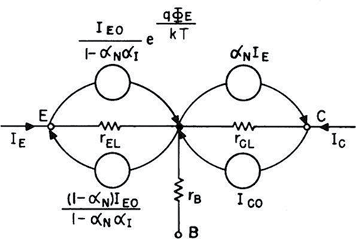
Figure 2. Fig. 5 of [6], from 1954. ϕE is the base-emitter bias VBE. The quantities subscripted O are parameters, αN and αI are normal (forward, IC/IE) and inverted (reverse, IE/IC) current “gains.”
Compact modeling changed drastically with the arrival of circuit analysis programs in the 1960’s, followed by the evolution of circuit simulators in the 1970’s. Early circuit analysis programs include ECAP from IBM [7] and NET-1 from the Los Alamos National Lab [8]. At about the same time, R. K. Jensen published a paper describing his implementation of the Ebers-Moll model, in ECAP, for DC and transient analysis [9].
Combining circuit simulators and compact models had an immense effect on the design community. On the one hand, simplicity was not as relevant, since it was no longer the designer who had to evaluate the device equations. Compact models could therefore include greater complexity to provide a more physical representation of the device. On the other hand, including compact models in a circuit simulator proved to be a difficult task. Simulation algorithms require that the device equations for current, charge, and flux be continuous with respect to voltage, and the algorithms work better if the first derivatives are continuous as well. There is also the tradeoff of accuracy of a model versus the computational complexity of the model. Finally, compact modeling came to require a reasonable knowledge of how circuit simulators work and how to implement a model in a simulator. This was a daunting task for circuit designers and device physicists who were unfamiliar with computer programming. These issues persist in the compact modeling world to this day.
IV. Empirical Compact Models
Notwithstanding the pioneering pn-junction diode and JFET models from Shockley, when it came to the bipolar junction transistor (BJT, which Shockley invented after the point-contact transistor of Bardeen and Brattain 75 years ago), the theory lagged a bit.
Experimentally, it was observed that the collector current IC of a BJT was (closely) proportional to the emitter current IE over many orders of magnitude of current; the ratio of those currents is now universally known as the quantity α. This observation, along with the Shockley relation (1), was the basis of the Ebers-Moll BJT model [6]. While the Ebers-Moll model was, for its time, quite “physical,” through the lens of history it missed the fundamental physics that underlies BJT operation.
Many data-driven approaches to modeling for circuit simulation have been, and continue to be, used. These include interpolation, a.k.a. table-based, models [10], and neural networks [11]. In the power RF community such approaches are considered to be “compact” models [12]; in the broader IC design community they are not [13].
V. Physical Compact Models: Hermann Gummel Sets the Path to the Future
While empirical compact models can be quick to generate, they have some drawbacks; it is difficult to include
- global statistical variation
- local statistical variation (i.e., parametric mismatch)
- geometric scaling, including layout dependent effects (LDEs)
- temperature variation, including self-heating
- fundamental requirements like smoothness, monotonicity, and symmetry
For these reasons, compact models based on physical (structural and layout) parameters and physics-based analysis are today the norm, and in fact all industry standard models from the Compact Model Coalition (CMC) [14] are physical, not empirical, compact models.
The guiding light, the archetype, for all modern compact models is the Gummel-Poon (GP) model for BJTs [15], which is based on the Gummel integral charge-control relation (ICCR) [16]. The collector-emitter transport current is
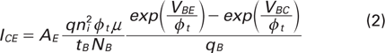
where AE is the emitter area, ni is the intrinsic concentration, and tB and NB are the thickness and doping of the base, respectively. The normalized base charge qB (details not shown) embodies both modulation by the bias dependence of the depletion region edges in the base (the Early effect [17]) and modulation by high-level injection.
Figure 3 shows the effect of qB; how this is included in modern BJT models was pioneered in [15], which was a work of sheer genius.
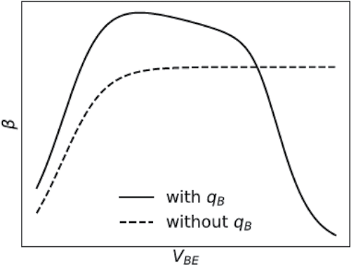
Figure 3. BJT current gain β = IC/IB from (2) with and without the qB term included. The behavior with qB is physically correct, the behavior without qB, which is exhibited by the empirical Ebers-Moll model, is not physically correct.
Once you understand (2) you understand how BJTs work. That is the power of a physical, intuitive, compact model.
VI. MOS Transistor Compact Models
Given the importance of CMOS technology today, it is perhaps surprising how long, tortured, and fractured the development path is to modern MOS transistor models.
MOS transistors come in several flavors, including: bulk (planar), silicon-on-insulator (SOI), dual-gate, tri-gate, and gate-all-around (a.k.a. nanowire or nanosheet) transistors. The basic operation of all is the same: an electric field (from the applied gate bias) transverse to the surface, whatever the device structure, induces a conducting channel, and a longitudinal electric field (from the applied drain-source bias VDS) drives current through the induced conducting channel.
There are 5 general classes of MOS transistor models:
- threshold voltage (VT) based models
- inversion charge based models
- surface potential based models
- the virtual source (VS) model
- the Taur approach for dual-gate MOS transistors
The first of these is probably the most familiar, as it is how MOS transistor operation is taught in most undergraduate classes and design textbooks. From [18] the drain current in a planar MOS transistor is

where W and L are the transistor length and width, respectively,  is the oxide capacitance per unit area, and VT is the threshold voltage, which depends on the voltage w.r.t. the body. The BSIM4 model [19] represents the pinnacle of development of VT based models, and has been used for the design of more ICs than any other MOS transistor model. However, the drain/source symmetry inherent in (3) was lost over the years, which caused significant issues for simulation of RF CMOS circuits, so VT-based models have fallen out of favor.
Models based on the (normalized) inversion charge density qi have been independently developed multiple times, starting in 1987 [20], and culminating in BSIM-BULK [21]. From the 10,000 m level, this approach posits that

where Vp is the pinchoff voltage and Vch is the “channel” voltage. The beauty of this formulation is that it naturally transistions from the approximate exponential variation of qi with gate bias in weak inversion to the near linear variation in strong inversion.
The surface potential approach is generally recognized as the most physically accurate formulation for MOS transistor modeling, and is also the basis of the CMC standard model for FinFETS [22]. It is too complex to summarize here, interested readers can digest the overview of [23].
A rather different approach to modeling MOS transistors is the “virtual source” formulation [24]. All FET models assume there is no recombination in the channel. Therefore, the product of the inversion charge density Qi(x) and the average carrier speed v(x) must be the same at every point along the channel. So, you only need to model those quantities at one point along the channel to characterize the behavior of the whole transistor. Fig. 4 shows how this approach works: xo is the position along the channel of the virtual source, so Qi and v at that point are used to model ID.
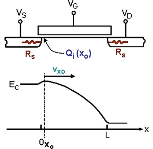
Figure 4. Fig. 1 of [24], virtual source view of MOS transistor operation.
An innovative approach to modeling dual-gate transistors was pioneered by Yuan Taur [25]. This approach, unlike the other approaches listed above, has not been adopted in any CMC standard model. But it is so different, and so elegant, it warrants attention.
Amazingly, most modern MOS transistor compact models (the exception being the VS model) are based on the “gradual channel approximation,” which was first introduced by Shockley for JFETs [5]. In a nutshell, this posits that to solve Poisson’s equation for the charge density in the channel, the longitudinal electric field can be ignored, and only the transverse electric field need be considered. Corrections for the inaccuracies of this approximation have been investigated [26], but the fundamental approximation of [5] is still the basis of modeling for all FETs.
VII. Compact Models for Other Devices
The models briefly outlined above are relatively simple. Probably the most complex devices to model are LDMOS transistors, for which modeling of the drift region, which allows them to sustain the high voltages necessary to interface to the real world, is at least as complex as modeling the core MOS transistor. The low-voltage digital circuits in our cars and phones have to interact with the real world at some point, and in many cases LDMOS transistors are the interface.
Even what we consider to be basic, simple devices such as capacitors and inductors are neither basic nor simple in modern ICs: their layouts are increasingly complex, and accuracy requirements for the models, over layout and frequency, continually escalate ... if they didn’t, your phone battery may die faster than it already does!
Even resistors are not simple: As undergraduates we are all indoctrinated that V = I • R, but integrated resistors are a bit more complex than that: their behavior is affected by depletion pinching, velocity saturation, and self-heating, and they are really JFETs [27].
VIII. Why Compact Models are Always Playing “Catch-up”
Compact models are vastly more accurate today than they were 75 years ago. But they are still imperfect; in several aspects embarrassingly so for model developers. With the increasing importance of LDEs and parasitics, and the inability of models to keep up with the cadence of technology development in these areas, there will always be “unsimulatable” effects.
The expectations of how accurate compact model are have continued to escalate, yet the gaps between simulation and reality, especially for compact models, have never been closed as more physical effects come into play and accuracy requirements have become more demanding. The Shichman-Hodges MOS transistor model [18] was revolutionary 50 years ago, but is completely inadequate for today’s needs. As technology continues to scale, what “fine details” of modeling bubble up to be make-or-break capabilities continue to evolve.
The expectations for compact models today are much, much more stringent than they were 75 years ago. Circuits have 108 more components, supply voltages are significantly smaller so sensitivity to variability is much greater, sensitivity to inaccuracies in models is vastly higher, and many more circuit performance characteristics are important. The capabilities of simulators and compact models have improved astronomically, but the complexity of the circuits that are simulated, and the expectations of the accuracy of those simulation results, have increased at a greater rate. So, basically, the algorithms and models in SPICE are continually playing catch-up.
The reality is that simulation algorithms and compact models have, despite huge steps forward, struggled to keep pace with the increasing expectations of how accurate they should be.
This is not a problem for expert IC designers. It is a huge problem, recognized in both industry and academia, for the “SPICE jockeys” who blindly run, and trust, SPICE simulation results. There is no substitute for knowledge of how circuits operate and of physical understanding of how devices behave.
Acknowledgment
An extended version of this article will appear in the commemorative volume, 75th Anniversary of the Transistor, IEEE Press-Wiley, 2023.
References
[1] L. W. Nagel, SPICE2, A Computer Program to Simulate Semiconductor Circuits. PhD thesis, EECS Department, University of California, Berkeley, May 1975.
[2] W. Shockley, Electrons and Holes in Semiconductors (With Applications to Transistor Electronics). New York, NY, USA: Van Nostrand, 1950.
[3] L. W. Nagel and C. C. McAndrew, “Why SPICE is just as good and just as bad for IC design as it was 40 years ago,” in 2018 48th European Solid-State Device Research Conference (ESSDERC), pp. 170–173, 2018. DOI: 10.1109/ESSDERC.2018.8486875.
[4] L. W. Nagel and C. C. McAndrew, “Is SPICE good enough for tomorrow’s analog?,” in 2010 IEEE Bipolar/BiCMOS Circuits and Technology Meeting (BCTM), pp. 106–112, 2010. 10.1109/BIPOL.2010.5668096.
[5] W. Shockley, “A unipolar “field-effect” transistor,” Proc. IRE, vol. 40, pp. 1365–1376, Nov. 1952. DOI: 10.1109/JRPROC.1952.273964.
[6] J. J. Ebers and J. L. Moll, “Large-signal behavior of junction transistors,” Proceedings of the IRE, vol. 42, no. 12, pp. 1761–1772, 1954. DOI: 10.1109/JRPROC.1954.274797.
[7] “1620 electronic circuit analysis program (ECAP),” Tech. Rep. 1620-EE-02X, IBM Corporation.
[8] A. F. Malmberg, F. L. Cornwell, and F. N. Hofer, “NET-1 network analysis program,” Tech. Rep. LA-3119, Los Alamos Scientific Laboratory, 1964.
[9] R. W. Jensen, “A charge control transistor model for the IBM circuit analysis program,” IEEE Transactions on Circuit Theory, vol. 13, pp. 428–437, Dec. 1966.
[10] J. Barby, J. Vlach, and K. Singhal, “Polynomial splines for MOSFET model approximation,” IEEE Transactions on Computer-Aided Design of Integrated Circuits and Systems, vol. 7, no. 5, pp. 557–566, 1988. DOI: 10.1109/43.3193.
[11] A. Zaabab, Q.-J. Zhang, and M. Nakhla, “A neural network modeling approach to circuit optimization and statistical design,” IEEE Transactions on Microwave Theory and Techniques, vol. 43, no. 6, pp. 1349–1358, 1995. DOI: 10.1109/22.390193.
[12] D. E. Root, J. Xu, F. Sischka, M. Marcu, J. Horn, R. M. Biernacki, and M. Iwamoto, “Compact and behavioral modeling of transistors from NVNA measurements: New flows and future trends,” in Proceedings of the IEEE 2012 Custom Integrated Circuits Conference, 2012. DOI: 10.1109/CICC.2012.6330642.
[13] C. C. McAndrew, “A perspective on RF modeling,” in IEEE 16th Topical Meeting on Silicon Monolithic Integrated Circuits in RF Systems, pp. 84–87, 2016. DOI: 110.1109/SIRF.2016.7445475.
[14] “Si2 compact model coalition.” https://si2.org/cmc/. Accessed: Dec. 2022.
[15] H. K. Gummel and H. C. Poon, “An integral charge control model of bipolar transistors,” Bell Syst. Tech. J., vol. 49, pp. 827–852, May-Jun. 1970. DOI: 10.1002/j.1538-7305.1970.tb01803.x.
[16] H. K. Gummel, “A charge control relation for bipolar transistors,” Bell Syst. Tech. J., vol. 49, pp. 115–120, Jan. 1970. DOI: 10.1002/j.1538-7305.1970.tb01759.x.
[17] J. M. Early, “Effects of space-charge layer widening in junction transistors,” Proceedings of the IRE, vol. 40, no. 11, pp. 1401– 1406, 1952. DOI: 10.1109/JRPROC.1952.273969.
[18] H. Shichman and D. A. Hodges, “Modeling and simulation of insulated-gate field-effect transistor switching circuits,” IEEE J. Solid-State Circuits, vol. 3, pp. 285–289, Sep. 1968. DOI: 10.1109/JSSC.1968.1049902.
[19] N. Paydavosi, T. H. Morshed, D. Lu, W. Yang, M. V. Dunga, X. Xi, J. He, W. Liu, K. M. Cao, X. Jin, J. J. Ou, M. Chan, A. M. Niknejad, and C. Hu, “BSIM4v4.8.0 MOSFET Model Users’ Manual.” http://www2.eecs.berkeley.edu/Pubs/TechRpts/1973/22871.html, 2013. Accessed: Sep. 2019.
[20] M. A. Maher and C. A. Mead, “A physical charge-controlled model for MOS transistors,” in Advanced Research in VLSI (P. Losleben, ed.), Cambridge, MA, USA: MIT Press, 1987.
[21] H. Agarwal, C. Gupta, H.-L. Chang, S. Khandelwal, J. P. Duarte, Y. S. Chauhan, S. Salahuddin, and C. Hu, “BSIM-BULK106.2.0 MOSFET Compact Model Technical Manual.” https://bsim.berkeley.edu/models/bsimbulk/, 2017. Accessed: May 2020.
[22] S. Khandelwal, J. Duarte, A. S. Medury, S. V., N. Paydavosi, D. Lu, C. Lin, M. Dunga, S. Yao, T. Morshed, A. Niknejad, S. Salahuddin, and C. Hu, “BSIM-CMG 110.0.0 Multi-Gate MOSFET Compact Model Technical Manual.” http://bsim.berkeley.edu/models/bsimcmg/, 2015. Accessed: May 2020.
[23] G. Gildenblat, W. Wu, X. Li, R. van Langevelde, A. J. Scholten, G. D.-J. Smit, and D. B. M. Klaassen, “Surface-potential-based compact model of bulk MOSFET,” in Compact Modeling: Principles, Techniques and Applications (G. Gildenblat, ed.), ch. 1, pp. 3–40, New York, NY, USA: Springer, 2010. DOI: 10.1007/978-90-481-8614-3.
[24] A. Khakifirooz, O. M. Nayfeh, and D. Antoniadis, “A simple semiempirical short-channel MOSFET current-voltage model continuous across all regions of operation and employing only physical parameters,” IEEE Trans. Electron Devices, vol. 56, pp. 1674–1680, Aug. 2009. DOI: 10.1109/TED.2009.2024022.
[25] Y. Taur, X. Liang, W. Wang, and H. Lu, “A continuous, analytic drain-current model for DG MOSFETs,” IEEE Electron Device Letters, vol. 25, pp. 107–109, Feb. 2004. DOI: 10.1109/LED.2003.822661.
[26] K. Mayaram, J. Lee, and C. Hu, “A model for the electric field in lightly doped drain structures,” IEEE Transactions on Electron Devices, vol. 34, no. 7, pp. 1509–1518, 1987. DOI: 10.1109/TED.1987.23113.
[27] K. Xia and C. C. McAndrew, “JFETIDG: a compact model for independent dual-gate JFETs with junction and MOS gates,” IEEE Trans. Electron Devices, vol. 65, pp. 747–755, Feb. 2018. DOI: 10.1109/TED.2017.2786043.