Technical Briefs
Silicon Solar Cell Turns 70
Santosh Kurinec1 and John Perlin2
1Electrical & Microelectronic Engineering,
Rochester Institute of Technology,
2Department of Physics, University of California, Santa Barbara
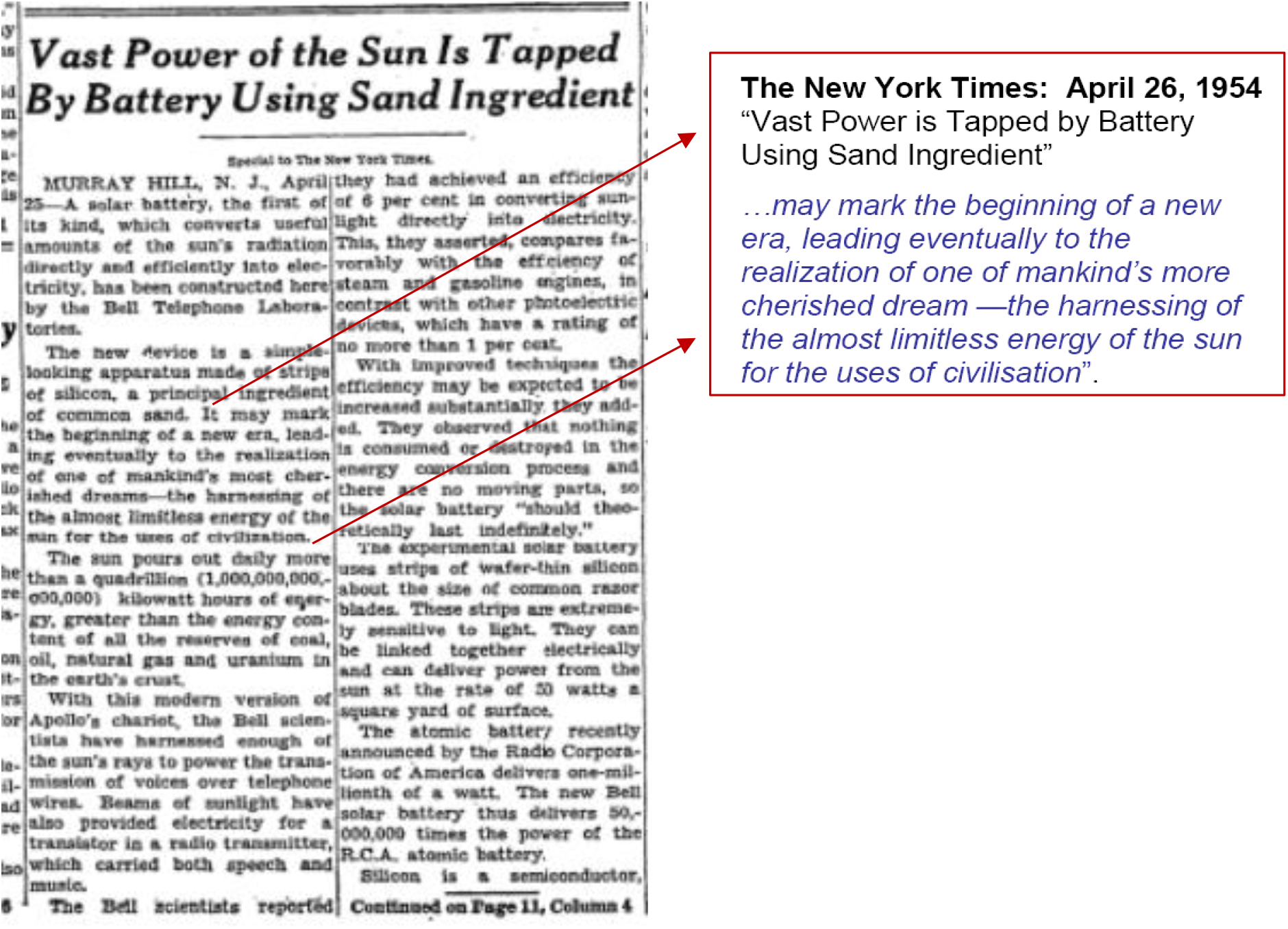
On 25 April 1954, Bell Labs in Murray Hill, New Jersey announced the invention of a silicon solar cell. They demonstrated their solar panel by using it to power a small toy Ferris wheel and a solar-powered radio transmitter. The New York Times on 26 April 1954 wrote that the silicon solar cell “may mark the beginning of a new era, leading eventually to the realization of one of mankind’s most cherished dreams–the harnessing of the almost limitless energy of the sun for the uses of civilization.”
The inventors Daryl Chapin, Calvin Fuller, and Gerald Pearson were simply trying to solve problems within the Bell telephone system to explore alternative sources of freestanding power. Selenium solar cells, the only type on the market, produced too little power—a mere 5 watts per square meter—converting less than 0.5% of the incoming sunlight into electricity. Calvin Fuller, a chemist, and Gerald Pearson, a physicist, were studying the properties of semiconductors by introducing impurities. They observed that when gallium-doped silicon was dipped in lithium, it resulted in a light-generated current, to their surprise. Observing the instability of lithium, they replaced it with arsenic to get a stable p-n junction. It yielded ∼ 6% conversion efficiency. That was the beginning of switching from selenium to silicon [1].
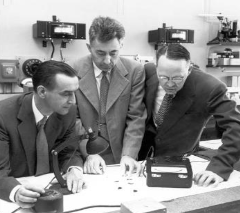
The inventors of the Si p-n junction Bell Solar Battery, from left, Gerald Pearson, Daryl Chapin, and Calvin Fuller, Credit: AT&T Archives.
In 1958, the American satellite Vanguard 1 entered orbit with six square silicon solar cells, (roughly 5 cm on a side) which generated about 1-watt power in total. Most PV interests in the US were for space applications. The IEEE started the first Photovoltaic Specialists Conference (also called PVSC) in 1961 at the NASA headquarters in Washington DC. It is the longest-running technical conference dedicated to photovoltaics, solar cells, and solar power.
Growing interest in re-evaluating terrestrial applications emerged with the release of small commercial modules by Sharp, Philips, and Solar Power in the early 1970s. The energy crisis and subsequent oil embargoes stimulated the rapid development of PV technology in the mid-1970s, with the first modern modules fabricated in 1976. In 1978, President Carter founded the Solar Energy Research Institute (SERI) in Golden, Colorado and later in 1991, President George H. W. Bush elevated SERI to a national member of the Department of Energy (DOE) - National Renewable Energy Laboratory (NREL). Martin Green, PV pioneer and world-leading specialist in both monocrystalline and polycrystalline silicon solar cells, founded in University of New South Wales (UNSW) Australia, Engineering, the largest and best-known university-based photovoltaic research group in the world in 1974 [2].
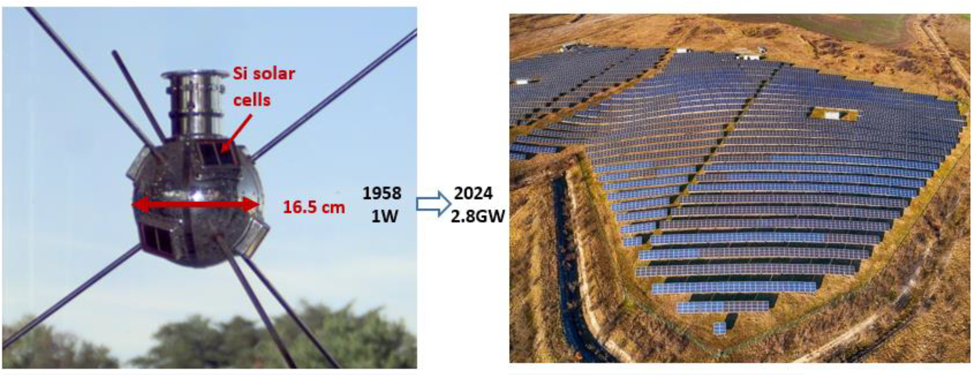
Vanguard 1 with its six solar cells attached (Source: Wikipedia)
2.8 GW Golmud Solar Park in China
(https://www.theecoexperts.co.uk/solar-panels/biggest-solar-farms)
The US DOE SunShot initiative was launched in 2011 with the goal of cost reduction of utility-scale solar to approximately $1 per watt- or $0.06 per kilowatt-hour that was met three years earlier in 2017. The program recently expanded its target to $0.03 per kilowatt-hour by 2030.
Crystalline silicon with a bandgap of 1.12 eV has the theoretical Shockley and Queisser efficiency limit of ∼ 29.4% [3]. Over the last seven decades, academics, scientific laboratories, and niche industries worldwide have remained diligently committed in achieving higher efficiencies across cell, module, and system levels. A series of high-efficiency crystalline silicon solar cell structures have emerged, that include passivated emitter rear cell (PERC), passivated emitter, rear locally diffused cell (PERL), interdigitated back contact cell (IBC), heterojunction with intrinsic thin-layer cell (HIT), heterojunction solar cells with interdigitated back contacts (HBC), bifacial cells and TOPCon solar cells. At the substrate level, monocrystalline silicon grown by the Czochralski method has dominated in efficiency and cost reduction by increasing the wafer size (210 mm × 210 mm) and decreasing the wafer thickness (∼170 μm). Cells have reached ∼ 27.5% in efficiency today. Detailed information on these innovations, co-authoring with Martin Green will be presented in IEEE Electron Devices Magazine. The efficiency has increased ∼ 0.3% per year since 1954 and worldwide silicon PV installations have exceeded terawatts. The Golmud Solar Park in China is the world’s largest solar farm at present with an installed solar capacity of 2.8 GW, with nearly seven million solar panels. Happy Birthday, Si Solar Cell!
Rochester IEEE EDS local chapter will celebrate the 70th birthday of Si Solar Cell at the Imagine RIT Festival dedicated to sharing scientific and technical achievements with the public on 27 April 2024.
References
[1] D. M. Chapin, C. S. Fuller, G. L. Pearson; A New Silicon p-n Junction Photocell for Converting Solar Radiation into Electrical Power. J. Appl. Phys. 1 May 1954; 25 (5): 676–677. https://doi.org/10.1063/1.1721711
[2] M. A. Green; Forty Years of Photovoltaic Research at UNSW. Journal and Proceedings of the Royal Society of New South Wales, vol. 148, nos. 455 & 456, pp. 2-14. ISSN 0035-9173/15/010002-13
[3] W. Shockley, H. J. Queisser; Detailed Balance Limit of Efficiency of p-n Junction Solar Cells. J. Appl. Phys. 1 March 1961; 32 (3): 510–519. https://doi.org/10.1063/1.1736034
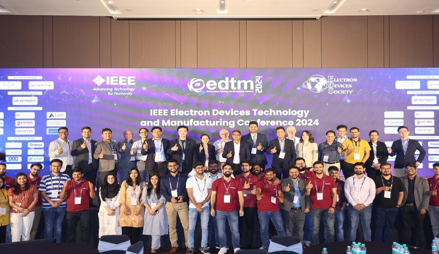
8th IEEE Electron Devices Technology and Manufacturing (EDTM) Conference
Introduction
Since its inception in 2017 in Toyama, Japan, IEEE Electron Devices Technology and Manufacturing (EDTM) Conference has been hosted by all the major Asian countries with semiconductor manufacturing hubs. The 8th edition of this conference was held in India for the first time at Bengaluru; the Silicon Valley of India and hub of semiconductor companies; preserving the tradition. IEEE EDTM 2024 was an in-person full four-day conference held between 3–6 March 2024 at the Hilton hotel Bengaluru Embassy Manyata Business Park. Promoting the theme of “Strengthening Globalisation in Semiconductors”, this conference was loaded with 6 plenary talks, more than 145 keynote/invited talks, 140 accepted oral papers, over 107 accepted poster presentations with proceedings, and 60 accepted poster presentations without proceedings. In addition to the technical sessions, EDTM began with tutorials and short courses specifically designed to provide participants with in-depth knowledge and hands-on experience on advanced topics related to electron device technology and manufacturing. The conference was attended by over 600 participants from around 20 countries from all over the world, including US, UK, Spain, India, Belgium, Netherlands, Bangladesh, Austria, Australia, Russia, France, Saudi Arabia, Japan, and Taiwan. 26 national and international sponsors including 11 exhibition stalls embraced the event with their presence.
Day-wise details of the 2024 IEEE EDTM conference are presented below.
Day 0 (3 March)—Tutorials and Short-courses
The day prior to the technical sessions i.e. 3 March was dedicated to Tutorials and Short-courses which were conducted by the leading experts in the field from both industry and academia. EDTM 2024 offered 4 tutorials and 3 short-course sessions designed to provide in-depth insights and hands-on experience on specific topics of interest. These sessions allowed attendees to gain practical knowledge and skills in areas such as device fabrication techniques, simulation tools, and emerging technologies. Topics of the tutorials and their details are given below:
Tutorial 1: Wide Bandgap Devices for RF and Power Applications
GaN Power Transistors: Technology and Applications by Ken Shono; Transphorm Japan.
In this tutorial, structure, benefit, quality & reliability, and application of GaN were presented. There are two types of GaN in the market. One is Cascode GaN, another is p-GaN E- mode. A comparison of the two types was given. SiC is already in the market as high high-efficiency power switch. Pros and Cons of GaN and SiC were also discussed.
GaN Microwave/RF Transistors: From Fundamentals to Emerging Trends by Digbijoy Nath, Indian Institute of Science Bangalore, India.
This tutorial was dedicated to the basics of GaN RF HEMT keeping the focus on practical issues that are relevant for technology such as the effect of substrate, dislocations, compensation doping, device dimensions, passivation, etc. It was also discussed how various device dimensions and material/device properties affect device parameters, and how those, in turn, affect the performance of a power amplifier. How the device design and various aspects of it evolve with the need for power at higher frequencies, was also touched upon. Next, the lecturer discussed the transition to multi-finger HEMTs with high absolute output power because these are the devices that go into real-world systems. Since most research publications and reports on GaN HEMTs concern two-finger devices only, a large part of the know-how on how to realize multi-finger GaN RF HEMTs is often strategic in nature and also proprietary, and hence, not published. Finally, emerging trends in GaN RF devices were discussed in relation to the literature. These include GaN on silicon for low-power applications - especially E-mode devices, N-polar GaN for W-band, ultrathin barrier and buffer-free HEMTs, and approaches to realizing GaN HEMTs with better linearity. Future challenges and opportunities for GaN HEMT were also discussed.
Tutorial 2. Reliability in Advanced Semiconductor Devices
A Device to Circuit Framework for Aging (BTI, HCD) in Advanced Technology Nodes by Souvik Mahapatra, IIT Bombay, India.
In this tutorial, the following topics were discussed;
Insulators for Devices based on 2D Materials by Tibor Grasser, Institute of Microelectronics, TU Wien, Austria.
The selection of suitable insulators for 2D nanoelectronics has always been a challenge. this tutorial addressed the current state of the art and summarized the main problems together with potential solutions. This problem is of key importance since scaling of 2D semiconductors towards sub-10 nm channel lengths is only possible with gate insulators scalable down to sub-1 nm equivalent oxide thicknesses (EOT). To achieve competitive device performance, these insulators need to meet stringent requirements regarding (i) low gate leakage currents, (ii) low density of interface traps, (iii) low density of border insulator traps, and (iv) high dielectric strength.
The insulators typically used for 2D electronic devices are amorphous 3D oxides known from Si technologies (SiO2, HfO2, Al2O3), while native 2D oxides (MO3, WO3, and Bi2SeO5), layered 2D crystals (hBN, mica) and ionic 3D crystals (CaF2 and other fluorides like SrF2, MgF2) have received increasing attention. 3D oxides often form poor-quality interfaces with 2D semiconductors and contain border traps which severely perturb stable device operation. Native oxides, on the other hand, are often non-stoichiometric due to the lack of well-adjusted oxidation methods and thus have limited dielectric stability and inherently narrow bandgaps. As the most popular candidate, the layered 2D insulator hBN forms excellent van der Waals interfaces with 2D semiconductors but has mediocre dielectric properties resulting in excessive leakage currents for sub-1 nm EOT. The potential of other 2D insulators (e.g. mica) is currently unclear, in part due to the absence of scalable growth techniques. Finally, very promising insulators for 2D electronics are 3D ionic crystals like CaF2 which form well-defined interfaces to 2D channel materials. In contrast to hBN, fluorides have good dielectric properties and thus exhibit low gate leakage currents.
Tutorial 3. Artificial Neural Networks
In-Memory Computing for Artificial Neural Networks by Abu Sebastien, IBM Research Zurich, Switzerland.
This tutorial introduced Analog In-Memory Computing (AIMC) using non-volatile memory technology, emphasizing key concepts and related terminology. Following that, it presented a multi-tile mixed-signal AIMC chip designed for deep learning inference. Fabricated using 14nm CMOS technology, this chip features 64 AIMC cores/tiles built on phase-change memory technology. This presentation served as a foundation to explore the device, circuitry, architectural, and algorithmic aspects of AIMC in more detail. A key focus was on achieving classification accuracy equivalent to floating point precision while conducting the majority of computations in the analog domain with relatively lower precision. At the end, the tutorial discussed ongoing research efforts aimed at the next generation of AIMC chips and offered insights into the future outlook of this technology.
Biologically Realistic Artificial Neural Networks by Veeresh Deshpande, IIT Bombay, India.
The tutorial introduced the basics of piking neural networks (SNNs) highlighting the bio-realistic elements in their implementation and some of the learning/training mechanisms employed. The speaker briefly touched upon SNN hardware implementation examples, implementation of quantum tunneling-based neurons, and SNN implementation in 45 nm CMOS technology. Thereafter, various approaches and examples of the implementation of neurons, synapses, and SNNs with unique properties of nanoscale non-volatile memory (NVM) devices in hybrid CMOS-NVM technology were discussed. The talk was concluded by discussing challenges and opportunities for NVM-based implementation of SNNs.
Tutorial 4. TCAD and Compact Modeling
Compact Modeling: General Introduction and Modeling of Statistical Variability by Gert-Jan Smit, NXP Semiconductors, The Netherlands.
This tutorial started with a general introduction to compact modeling which included the role of compact models in the design flow, challenges related to their development, and a quick overview of the main compact models that are used in the industry today. Then, the presentation elaborated on the variability that inherently comes with semiconductor manufacturing. Accounting for this variability during circuit design is critical for the development of products with good fabrication yield. Consequently, it is critical that SPICE libraries not only accurately reflect the nominal behavior of the electrical components, but also capture the stochastic variations. It also reviewed, the most used methods to model variability in industrial SPICE libraries: fixed corners and Monte Carlo models. What are they based on, how are these models created, what modeling techniques are used, what do they represent, and - very importantly - what do they not represent? Special attention was devoted to the intrinsic limitations of corner models. Finally, the speaker discussed some lesser-known domains where variability modeling is very important: 1/f noise and (passive) backend devices.
MOSFET Characterisation and Modeling for Cryogenic Applications by Thomas Bedecarrats, CEA-Leti, Grenoble, France.
This tutorial provided an overview of today’s measurement methods, the latest reported cryogenic electrical behaviours, and corresponding compact modeling strategies. Finally, it discussed what is missing to get an operational PDK for IC design.
TCAD-based Compact Model Parameter Extraction of Si and SiC High-Power Devices by Vinay Kumar, Synopsys, India.
In this tutorial, the steps w.r.t. Process and Device simulation of power devices using Sentaurus TCAD – simulation of device characteristics required for extracting the model parameters of a given compact model were discussed in detail. The compact model could be a standard model approved by CMC for high-voltage power devices or a user-defined model based on a sub-circuit modeling approach. In the end, the speaker elaborated on the validation aspects of the compact model before using it for the circuit design tasks.
Short courses
Along with the tutorial sessions, short courses were conducted on the same day by experts in the field.
Short Course 1. Advances in Logic Devices
Logic Technology Roadmap by Gaurav Thareja, Applied Materials, USA.
This short course focused on the logic technology roadmap. The current state of transistors and interconnects, materials/process/equipment challenges, and emerging technologies for next-generation low-power, high-performance computing were explored. With FinFET scaling approaching its limits, innovative device architectures emerge as promising candidates for next-generation transistor technology, including Gate-All-Around (GAA) and complementary FET (CFET). To address large wire delay and the high IR drop issue resulting from continuous area scaling, novel interconnect material and innovative integration schemes like Backside Power Delivery Network (BSPDN) have been developed. It was also discussed why the technology roadmap follows a ‘perseverant tortoise’ approach and how we can expedite this.
Nanosheet-based Transistor Architectures for Advanced CMOS Scaling by Hans Mertens, IMEC Leuven, Belgium.
This short course covered various aspects of nanosheet-based transistor fabrication. The basic building blocks of GAA nanosheet fabrication were visualized by 3D animations. Subsequently, potential solutions to either place nanosheet-based transistors closer to each other (Forksheet) or stack them on top of each other (CFET) were described. Recent progress in the fabrication of these types of transistors was discussed, covering front-end-of-line and middle-of-line innovations.
Short course “Advances in Logic Devices/Logic Technology Roadmap” by Hans Mertens.
Short Course 2. Advances in Memory Technologies
DRAM and NAND Memories: Technology and Design Perspectives by C. R. Parthasarathy, Micron Technology, India.
This short course covered the fundamentals of the NAND and DRAM memories. The basics of technology and the devices associated with these memories were examined. The issues of scaling and design that provide exciting opportunities to create next-generation memory systems were also addressed.
DRAM Scaling: History and Innovation by Sungho Jang, Samsung Electronics, South Korea.
This course introduced the evolution and challenges of DRAM cell technology for DRAM scaling to increase its capacity. The future directions of scaling technology and topics such as overcoming data sensing margin challenges and the DRAM peripheral transistor technology challenges for achieving high performance of graphic DRAM (GDDR), and high-bandwidth memories (HBM) for AI servers in the era of sub-15 nm deep scaling were also discussed during this course.
Short Course 3. Semiconductor Packaging Technology
Recent Advancements in Interconnect Materials and Technologies in Semiconductor Packaging by Nilesh Badwe, Indian Institute of Technology Kanpur, India.
This course covered the advancement in both the first-level interconnects (FLI) and second-level interconnects (SLI) in semiconductor packaging. The FLIs have evolved from older generation techniques like wire bonding or flip chip using soldering to solderless direct copper-to-copper hybrid bonding enabling sub-10 µm pitch with significant improvement in performance. The course also highlighted the progress in the SLI connections with a case study on low-temperature solders for board-level assembly.
Day 1 (4 March): Inauguration Day
The inauguration started with welcoming all the participants including Plenary, Keynote, and Invited speakers by Prof. Yogesh Singh Chauhan (General Chair, EDTM 2024) and Prof. Mayank Shrivastava (General Co-chair, EDTM 2024). This was followed by the presentation of the Technical Program Committee report by Prof. Nihar Ranjan Mohapatra (TPC Co-Chair, EDTM 2024).
The crowning moment of the Inauguration session was conferring the Life-time Achievement Award to Prof. Juzer Vasi for his immense contribution to Indian micro/nanoelectronics research, known for sowing the seeds of microelectronics education in India. The IEEE EDS Early Career award was also given to Prof. Shubham Sahay from IIT Kanpur.
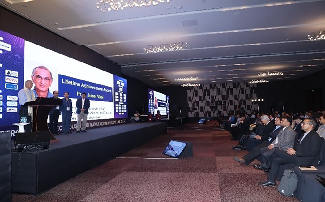
Conferring the Life-time Achievement Award to Prof. Juzer Vasi.
Following the inauguration session, the first plenary talk Semiconductor – the Next 75 Years? was given by Prof. Chenming Hu (TSMC Distinguished Professor Emeritus, University of California Berkeley, USA). He summarized the past 50 year history of semiconductor research and how it has contributed to the digital age lifting up the technology, industry, and even science. The second plenary talk GaN Technology enabling Power Electronics was given by Sameer Pendharkar (Vice President Technology Development and TI Senior Fellow, Texas Instruments, USA). 25 parallel sessions including 15 keynote, 47 invited and 38 oral presentations were witnessed by the participants on the first day of the conference covering the topics of CMOS Technology Scaling, RF, Millimetre and Terahertz Technologies, Circuits and Systems, TCAD and Manufacturing, Emerging Memory Technologies, Ferroelectric Materials and Devices I, WBG Device Applications, Packaging Materials, 2D Sensors, Design Technology Co-Optimization I, Neuromorphic Computing I, TCAD Simulation, Ferroelectric Memories, 2D Materials and Devices I, High Power Device Reliability, Packaging—Mechanical Properties and Reliability, Microfluidics and MEMS Sensors, Technology for Future Chips, Semiconductor Device Characterization, Neuromorphic Computing II, TCAD and Device Modeling, Ferroelectric FETs, Neuromorphic Devices, SiC-based Power Devices, Memory and Metallization Reliability, Yield, and Manufacturing.
The first Evening Panel Discussion titled: Is there no scope for deep tech semiconductor start-ups in India? was moderated by Prof. Ramgopal Rao (BITS Pilani, India). It gathered the panelists Chandrasekhar Nair (Bigtec Private Ltd.), Suryaprakash Konnanuru (CTO, Ideaspring Capital), Shantanu Chaturvedi (VP, Transition VC), Dipanjan Gope (CEO, Simyog Technology Private Limited) who delved into challenges faced by semiconductor start-ups in India and measures to be adopted to overcome them.
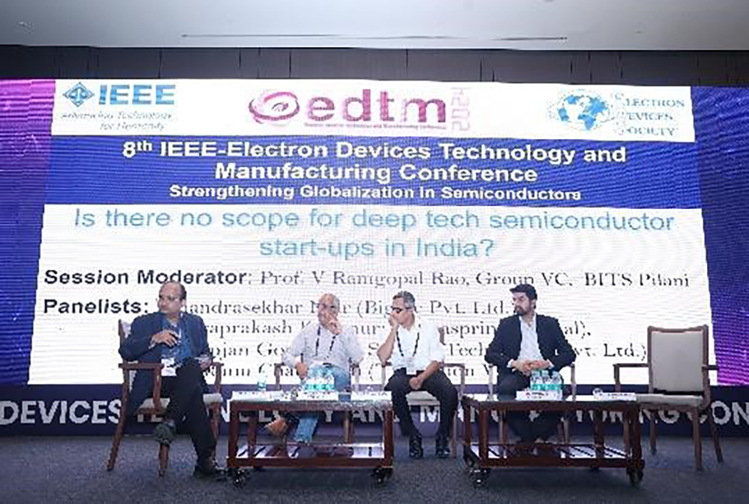
Panel Discussion titled: Is there no scope for deep tech semiconductor start-ups in India?
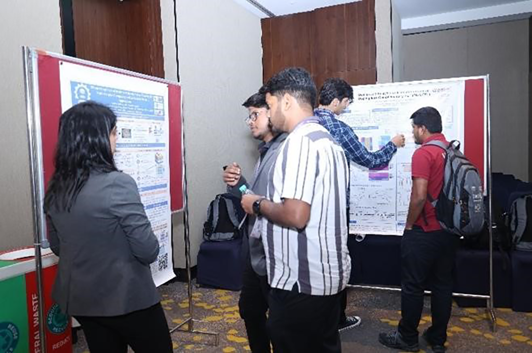
The latter half of the evening was devoted to the poster session I and IEEE Young Professionals Event. 167 posters were displayed for the viewers on day 1 and 2 of the conference, giving the opportunity for the students and researchers to showcase their work and share recent developments.
The IEEE Young Professionals event was attended by over 30 persons. The panel session gathered the speakers: Prof. Francesca Iacopi (FIEEE, Editor-in-Chief, IEEE Trans. Materials for Electron Devices), Early Career awardee, Prof. Shubham Sahay (IIT Kanpur), Prof. Avirup Dasgupta (IIT Rorkee), Prof. Manan Suri (IIT Delhi), Prof. Harshit Agarwal (IIT Jodhpur), Prof. Abhronil Sengupta (Penn State University) who generously shared their insights and suggestions with young researchers. That will help them advance their research towards real-world applications.
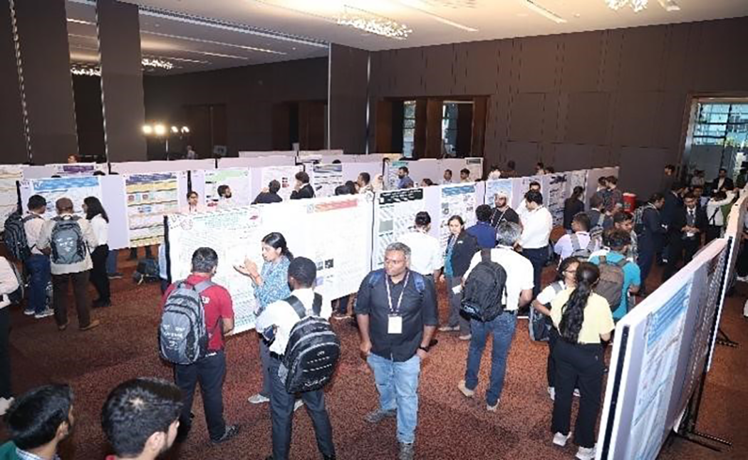
A view at the poster session
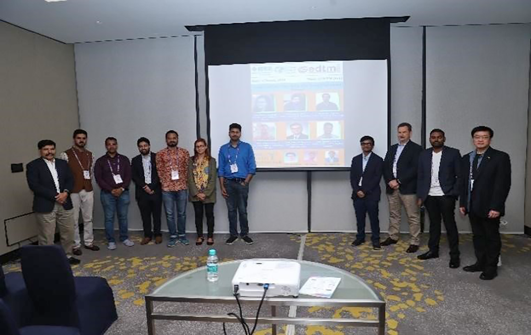
Participants of IEEE Young Professionals event with Bin Zhao, EDS President.
Day 2 (5 March)
The second day of the conference commenced with the third plenary talk by Dr. Balajee Sowrirajan (Samsung Electronics, India) titled: Semiconductor Systems Driving AI. It was dedicated to strengthening the globalization of semiconductors and advancing technology for the benefit of humanity. Highlighting the rapid progress of Generative AI in the semiconductor industry, the speaker emphasized its transformative impact and discussed its applications in areas like TextToText, TextToImage, ImageToText, and beyond. He also delved into the rapidly changing landscape of coding, where various tools are gaining momentum.
The fourth plenary talk From Ferroelectric Materials to Enhanced Semiconductor Devices was delivered by Prof. Thomas Mikolajick (NaMLab GmbH, Germany). As a leading figure in the field of ferroelectric memory and devices, he enriched the audience with the 100-year history of ferroelectric memories to its future opportunities and related challenges.
25 parallel sessions consisting of 38 invited talks, 12 keynote, and 62 oral presentations were devoted to the following topics: Gate-All-Around (GAA) Devices, In-Memory Computing I, Cryogenic CMOS Compact Modeling, 2D Materials and Devices II, AI/ML in Process Control, Package Manufacturing, Logic, Memory and 2D Material Reliability, Si; SiGe, III-V Technologies for RF Applications, Alternate Devices and Computing Options, Flash Memories, Ab-initio Simulation and Modeling, Thin Film Devices, Sensors and Biosensors I, Integrated Photonics I, Ga2O3-based Power Devices, SOI Devices for RF Applications, Ferroelectric Materials and Devices II, Unconventional Computing I, Design Technology Co-Optimization II, Optoelectronic Devices, Sensors and Biosensors II, Integrated Photonics II, Solar Cells, and GaN HEMTs for RF Applications.
Apart from the poster session, the evening of the second day was reserved for the IEEE WiED event. That interesting session is broadly reported in the EDS Women in Engineering section of this Newsletter issue.
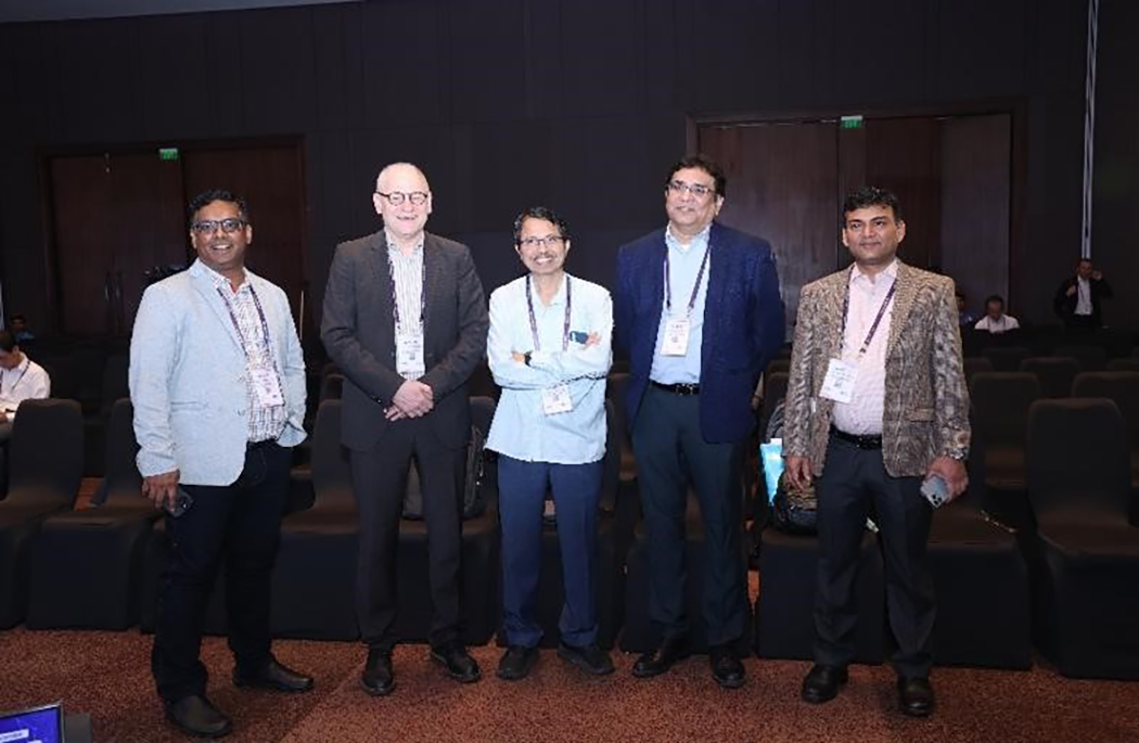
From the left: Prof. Nihar Ranjan Mohapatra, Prof. Thomas Mikolajick, Prof. Navakanta Bhat, Dr. Balajee Sowrirajan, and Prof. Yogesh S. Chauhan before the plenary session on the 2nd day of the conference.
The Evening panel discussion titled: Is Quantum the new Nano? had panelists: Manish Chhowala (University of Cambridge, UK), Ritesh Agarwal (University of Pennsylvania, USA), Hitoshi Wakabayashi (Tokyo Institute of Technology, Japan), Samit Ray (IIT Kharagpur, India) and was moderated by Saptarshi Das (Pennsylvania State University, USA).
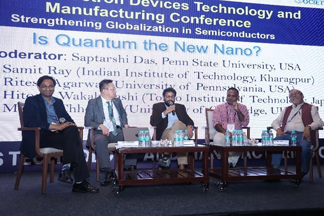
The Evening panel discussion: Is Quantum the new Nano?
Day 3 (6 March)
Two eminent experts gave plenary talks on the 3rd day of the conference Firstly, Anand Murthy (Intel, USA) presented the topic Transistor Scaling for the Future. As transistor sizes shrink, power density rises, leading to issues such as increased heat generation and power inefficiency. Overcoming the Power Wall is crucial for sustaining advancements in technology and preventing devices from becoming impractical due to excessive energy consumption. Intel Corporation as a leading technology enabler is coming up with a series of innovations to address this challenge for the future. The last plenary talk of the conference was given by Srinivas Raghvendra (Synopsys, USA) and was titled Simulation and Analytics in the Angstrom Era. The speaker emphasized the transition from the nanometer scale to the angstrom one in semiconductors, and how the electronics industry can make the best of it.
15 parallel sessions with 27 invited talks, 5 keynote talks, and 46 oral presentations were held on the 3rd day. They covered the following topics: Design Technology Co-Optimization III, In-Memory Computing II, ML-based Device Modeling, RRAM and OTS Selected Crossbar Arrays, 2D Materials and Devices III, Process and Metrology, Package Design, Printed Devices, GaN-based Power Devices, In-Memory Computing III, Ferroelectric/Memory Modeling, Unconventional Computing II, Magnetic, Straintronic and Quantum Computing Devices, and MEMS Devices.
Student Research Forum (SRF)—To promote and encourage young researchers in the domain of semiconductor devices and circuits, a Student Research Forum (SRF) was also organized during the last day of the conference. This forum helped students interact with the pioneers in their research area and get valuable feedback on their work, where 12 students presented their work through posters.
Participants of the Student Research Forum
The conference concluded with the closing remarks and awards ceremony. A vote of thanks was given by Yogesh Singh Chauhan (General Chair, EDTM 2024) and Mayank Shrivastava (General Co-chair, EDTM 2024).
Awards
EDTM 2024 recognized outstanding contributions with Best Paper Awards. The awards honoured researchers whose work demonstrated exceptional quality, significance, and impact in the field of electron devices technology and manufacturing. The awards were presented by Bin Zhao, EDS President. Congratulations to the recipients of this prestigious recognitions. Details of the awards are given below:
Best Student Research Forum (SRF) Poster Award:
Best Poster Awards:
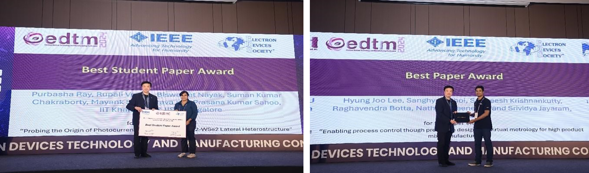
Bin Zhao, EDS President presenting the Best Student Paper Award (left ) and the Best Paper Award (right).
The EDTM 2024 conference is over; we are looking forward to meeting you at EDTM 2025.
Best Student Paper Awards:
Best Paper Award:
Conclusion: Overall, the IEEE Electron Devices Technology and Manufacturing Conference (EDTM) 2024 was a resounding success, providing a platform for advancing the frontiers of electron devices technology and manufacturing. The conference fostered collaboration, knowledge exchange, and innovation, contributing to the continued growth and evolution of the field. We look forward to future editions of EDTM and the exciting developments they will bring.
The 9th IEEE Electron Devices Technology and Manufacturing (EDTM) Conference, 2025 is scheduled on 9–12 March 2025 at Hong Kong Science and Technology Parks (HKSTP) as announced by Shuji Ikeda (TEI Solutions).
Yogesh Singh Chauhan (General Chair)
Mayank Shrivastava (General Co-Chair)
Nihar Ranjan Mohapatra (TPC Co-Chair)
Shubham Sahay (Treasurer)