Technical Briefs
A Review of the 67th
IEEE International Electron Devices Meeting
The annual IEEE IEDM conference (www.ieee-IEDM.org), sponsored by the IEEE Electron Devices Society, is the world’s largest, most influential forum for the unveiling of breakthroughs in transistors and related micro/nanoelectronics devices. At IEDM each year, the world’s best scientists and engineers in nano/microelectronics gather to participate in a technical program.
The 67th IEEE IEDM was scheduled for 11–15 December 2021 at the Hilton San Francisco Union Square Hotel. The main theme of the 67th annual IEEE IEDM was “Devices for a New Era of Electronics: From 2D Materials to 3D Architectures.” The Conference was held in-person with online access to recorded content afterward.
“This year the IEEE IEDM conference features a rich collection of presentations on topics that are on everyone’s minds. Among them are the advent of 2D materials, the growing number and diversity of 3D architectural concepts, the rise of system/technology co-optimization, and the possible end of Moore’s Law. Breakthroughs in these and other areas will be presented and discussed, and ultimately will help the industry and society as a whole move forward,” said Meng-Fan (Marvin) Chang, IEDM 2021 Publicity Chair, IEEE Fellow, Distinguished Professor of Electrical Engineering at National Tsing Hua University, and Director of Corporate Research at TSMC. “New, fast-growing electronics applications often require novel semiconductor solutions,” said Srabanti Chowdhury, IEDM 2021 Publicity Vice Chair and Associate Professor of Electrical Engineering at Stanford University. “With 3D technologies offering many intriguing ways to get around scaling issues, they open up new and exciting possibilities for highly integrated systems with far greater capabilities,” she added.
When organizing the Conference, great emphasis was placed on educational opportunities. “As the COVID-19 pandemic has demonstrated, the world is becoming increasingly reliant on electronic technologies. The good news is that the IEDM Tutorials and Short Courses will provide attendees with the invaluable knowledge and information needed to advance the state-of-the-art in critical areas of the field,” said Meng-Fan (Marvin) Chang. “The opportunity to engage with the world’s technical leaders in these highly specialized areas is one of the hallmarks of the IEDM conference,” he added. “The IEDM Tutorials and Short Courses represent a great opportunity to explore evolving areas of the field, with topics that include novel materials and device types; advances in process and packaging technologies; new design approaches; and much more,” said Srabanti Chowdhury.
Except for the Tutorials and Short Courses, the Conference technical program included plenary and regular talks, the evening panel, focus sessions, a supplier exhibit, IEEE EDS award presentations and other events highlighting leading work in more areas of the field than any other conference. The events of the 67th IEDM are briefly reported below.
Tutorials
The five-day Conference program started on 11 December 2021 with six tutorials. The 90-minute Saturday tutorial sessions on emerging technologies have become a popular and growing part of the IEEE IEDM. They are presented by experts in the field to bridge the gap between textbook-level knowledge and leading-edge current research, and to introduce attendees to new fields of interest. The following tutorials were held during the time-frame of the 67th IEDM:
Short Courses
The IEDM program was continued with two short courses held on Sunday, 12 December 2021. In contrast to the tutorials, the full-day short courses are focused on a single technical topic. They offer the opportunity to learn about important areas and developments, and to network with global experts. The following two short courses were held during the time-frame of the 67th IEDM:
Plenary Session
The first point of the IEDM program on Monday, 13 December 2021 was a plenary session. Three plenary talks were delivered, namely:
The plenary session was followed by a number of regular sessions, focus sessions, an Evening Panel and a Career Luncheon. The most newsworthy sessions and papers are briefly presented below.
Focus Sessions
Five Focus Sessions on key emerging technologies covered a range of topics addressing the gaps, challenges and opportunities for new approaches and technologies, including system-level issues and requirements; benchmarks of current technologies; and R&D directions for the new materials, devices, circuits, and modeling/manufacturing/testing approaches needed:
3D stacking from the device to the package level is a growing trend that will enable the industry to move to larger, more densely integrated circuits and systems. It will benefit greatly from the ability to integrate heterogeneous technologies into one solution (e.g., CFETs, quantum technologies etc.), along with new approaches to inspection and metrology. These issues were addressed in the following talks:
This Session explored R&D directions concerning new materials, devices, circuits, manufacturing and packaging approaches for Quantum Computing. The following talks concerning these topics were delivered:
As integrated circuits became more powerful and offered more functionality, the line started to blur between where a device ended and where a circuit began. A need was seen to design devices and circuits synergistically, a move called design-technology co-optimization (DTCO). Now, taking the idea of synergistic design a step further, system-technology co-optimization (STCO) is a growing trend. The approach encompasses leading-edge 3D concepts and heterogeneous technologies, and it is essential to enable new ways of computing, and to optimize the performance of new computing systems. One example is computing-in-memory (CIM) for artificial intelligence (AI)-based applications. Where and how data is stored in a CIM architecture is critical to its performance. The presentations below were about these matters:
AI and new architectures make possible new types of sensors for a growing number of use cases. They were discussed in the talks listed below:
Topological materials, where the surface is conducting but the bulk portion of the material is an insulator, are being investigated for their potential to enable ultra-small devices. This very promising theme was discussed in:
Regular Sessions
Among the papers presented during the regular sessions held from 13–15 December, a few general tracks may be distinguished. These tracks are briefly characterized below. Noteworthy papers are briefly presented.
A. CMOS Technology: New Ways to Advance Moore’s Law
3D at the Device Level: CMOS transistors are built in a lateral, or horizontal, fashion, and countless advances over decades have shrunk their dimensions so that billions of them can now be put on a chip, in accordance with the predictions of Moore’s Law. But shrinking transistors further in order to boost chip performance and add new features is difficult and costly. Would orienting them vertically instead of horizontally save space and make it easier to extend the life of Moore’s Law?
Inspired by trench-based DRAM vertical access transistors, a team from IBM and Samsung described in Paper #26.1, how they turned transistor architecture on its side, with CMOS devices built using so-called Vertical-Transport Nanosheets (VTFETs) on bulk silicon and with a 45nm gate pitch. The vertical devices offer the opportunity for continued scaling because gate length and spacer size—two key elements which determine gate pitch (the distance between transistors)—can be optimized in ways that aren’t possible horizontally. Also, the VTFET devices promise to deliver outstanding operating voltage and drive current as a result of reduced electrostatic and parasitic losses (SS = 69/68 mV/dec and DIBL= <30 mV). To validate the concept, the researchers used the VTFETs to make functional ring oscillators (test circuits), which demonstrated ∼50% reduction in capacitance vs. a lateral design reference.
Exploring Buried Power Rails: Interconnect is the term for the layers of wiring which connect everything on a chip. There are many interconnect layers in today’s most advanced chips, resulting in many interconnections which take up space and introduce undesirable electrical effects like resistance and capacitance. One possible way to continue scaling is to reconfigure the interconnect so that it takes up less space. In current designs, the top interconnect layer is what routes power to a chips’ transistors. If this “power rail” could be built closer to them—in the substrate right beneath them—then the interconnect stack could be reduced in height, the number of interconnections could be reduced, and smaller chip architectures would result. But it isn’t clear which metals a buried power rail (BPR) should be made from in order to address electrical performance, and for manufacturability. In Paper #22.5, a team from Imec and ASM International discussed their experiments evaluating different metals both for the BPR itself and also for the low-resistance contacts needed between the BPR and the through-silicon-vias that run through a chip’s different layers. They said that for future 3 nm transistors, a tungsten BPR optimizes line and contact resistance, and for 1 nm and 2 nm devices, molybdenum (Mo) appears better for the BPR and ruthenium (Ru) for the via contacts.
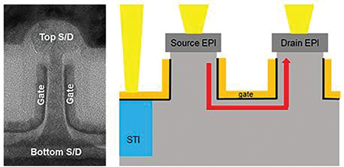
Paper #26.1, “Vertical-Transport Nanosheet Technology for CMOS Scaling beyond Lateral-Transport Devices,” H. Jagannathan et al, IBM/Samsung: left - a cross-sectional TEM of a VTFET nanosheet transistor (the source can be located at either the top or bottom for design flexibility), right - a schematic of an I/O device FET co-integrated with the VTFET
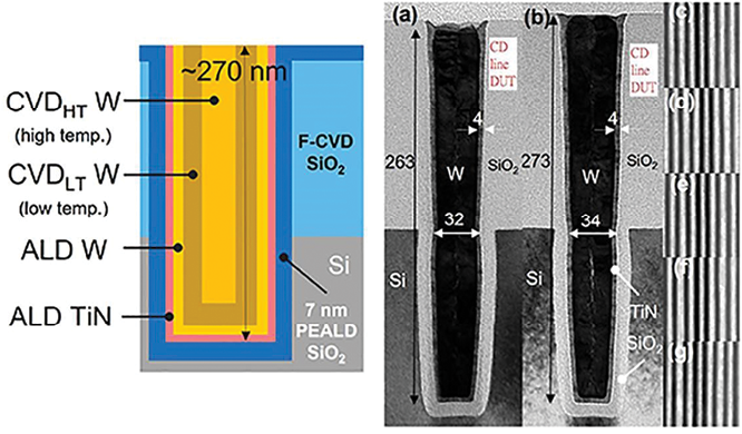
Paper #22.5, “Buried Power Rail Metal Exploration Towards the 1nm Node,” A. Gupta et al, Imec/ASM International: left—illustration of the tungsten (W) metallization stack (with a TiN liner used as an adhesion layer); right—the TEMs across the BPR line in (a) and (b) show the stack for on different wafers, and (c–g) shows void-free fill of lines for five different wafers
2D Materials Compatible With 300mm Production: Transition metal dichalcogenides (TMDs) are 2D materials with semiconducting properties. They are promising for use as the channel in highly scaled devices because they are <1 nm thick. However, much work is needed to understand the electron mobilities of various TMDs, the electrical resistance which metallic contacts impose on them, and other key aspects. In Paper #7.1 “Advancing 2D Monolayer CMOS Through Contact, Channel and Interface Engineering,” K.P. O’Brien/C. J. Dorow et al, Intel, the researchers reported fabrication and extensive studies of four TMD films: MoS2, WS2, WSe2 and MoSe2. The films demonstrated impressive performance, but most noteworthy is that all were grown at the 300mm scale in BEOL-type environments at process temperatures from 300 °C to 1,000 °C, meaning they are compatible with current mass-production methods.
Monolithic 3D Logic/Memory Integration for Machine Learning: As scaling becomes more difficult and expensive, the monolithic 3D integration of logic and memory is increasingly seen as a way to increase integration density, enrich the functionality and boost the performance of a single chip. A team of researchers from Tsinghua University and the Chinese Academy of Sciences described in Paper #21.5 their works on building a monolithic 3D device that combines 1) silicon CMOS logic; 2) a HfAlOx resistive-RAM (RRAM)-based computing-in-memory (CIM) layer; and 3) a complex ternary content-addressable memory (TCAM) layer. The device is intended for one-shot learning, which is a training technique for machine-learning applications. In one-shot tests using a standard data set, the device demonstrated a GPU-equivalent accuracy of up to 97.8% but with far lower energy consumption.
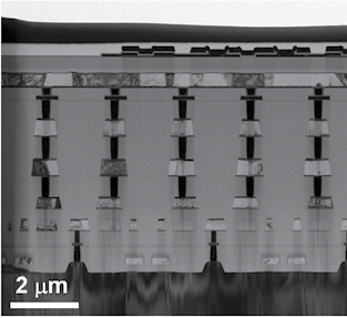
Paper #21.5, “Monolithic 3D Integration of Logic, Memory and Computing-In-Memory for One-Shot Learning,” Y. Li et al, Tsinghua University/Chinese Academy of Sciences: a cross-sectional TEM image of the 3D integrated chip
GaN Meets Moore’s Law: Gallium nitride (GaN) is a promising material for RF/mmWave and power applications, given its ability to operate at higher voltages and frequencies than silicon, and with lower losses. If GaN technology could be integrated effectively with CMOS technology and built using mainstream silicon CMOS tools and fabrication processes, then high-performance, energy-efficient and low-cost solutions could be created for next-generation PC/mobile devices, data centers, automotive radar, communication networks and other applications.
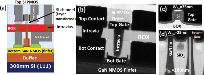
Paper #11.1, “Advanced Scaling of Enhancement-Mode High-K Gallium Nitride-on-300 mm-Si(111) Transistor and 3D Layer Transfer GaN-Silicon FinFET CMOS Integration,” H.W. Then et al, Intel: (a) a schematic of the 3D-stacked GaN-Si CMOS inverter; TEMs: (b) of the fabricated 3D layer-transfer stacked inverter, comprising a bottom GaN E-mode high-k NMOS FinFET transistor and a top Si PMOS FinFET transistor; (c) of the 35 nm-wide Si fin as the top PMOS channel; (d) of the 25nm-wide GaN fin as the bottom NMOS channel—this is the narrowest GaN fin with the highest aspect ratio (Hfin/Wfin = 7) ever demonstrated in literature
Intel researchers described in Paper #11.1 a highly scaled, high-performance, enhancement-mode high-k GaN-on-Si NMOS FinFET built on a 300 mm Si platform and integrated with Si PMOS FinFET technology. The heterogeneous device was made possible by a layer-transfer technique Intel first described at the 2019 IEEE IEDM that enables GaN NMOS and Si PMOS devices to be fabricated in parallel. The NMOS GaN FinFET features the narrowest GaN fin to date (width = 25 nm), an ultra-short gate length (30 nm), and is integrated with a Si PMOS FinFET having a fin width = 35 nm. The device achieved many industry firsts and records for GaN-on-Si, including a record fT/fMAX of 300/400 GHz and record transconductance (GM>2100 µS/µm) with the industry’s thinnest TOXE (14.8Å), among others. It is the first true enhancement-mode (i.e., “normally off”) GaN transistor with IOFF <25 pA/µm (up to VD = 30 V). The researchers demonstrated the technology by building a low-loss inverter with it. They said that going forward, GaN FinFET architectures and 3D layer-transfer technologies will play a significant role in GaN device scaling and in the ability to integrate more functionalities like CMOS with GaN technology.
B. Memory Technology
Significant Improvements in DRAM Reliability: Samsung researchers presented in the comprehensive Paper #6.6, “Reliability Characterization for Advanced DRAM using HK/MG + EUV Process Technology,” S. Lee et al, Samsung, demonstrating dramatic improvements in DRAM reliability at the 17 nm-to-15 nm technology nodes vs. the 18 nm node. This was achieved by transitioning to EUV for critical layers instead of using ArF immersion lithography; adopting HK/MG process technology for DRAM; and optimizing the gate dielectric breakdown of the buried access transistor (BCAT). A direct comparison of the breakdown voltage (Vbd) of test structures with EUV vs. immersion ArF demonstrated a clear improvement in low failure fractions for shorting nearest metal lines of the cell transistor, and a significant improvement in M0-to-metal contact process margin. High Temperature Operation Life (HTOL) testing exhibited a 2.2x reduction in failure rates for the 17 nm and 15 nm nodes. In order to confirm the success of their reliability improvements, the researchers tracked hundreds of thousands of DIMMs over one year of use, yielding a low cumulative failure of ∼100 ppm, a value consistent with their accelerated tests.
FeRAM with Record Performance for Embedded Memory: Hafnium-based ferroelectric RAM (FeRAM) stores memory bits in FE or AFE (antiferroelectric) capacitors by polarizing them electrically, versus storing bits in traditional capacitors as electrical charge, as DRAM memory does. FeRAM technology is promising as an embedded memory technology because it is highly scalable, high-speed, low-voltage and CMOS-compatible, and doesn’t require the use of low-leakage transistors as DRAM-based embedded memory does. Intel researchers described in Paper #33.2 how they built FeRAM with deep-trench AFE capacitors that showed industry-leading performance (read/write speed of ∼2 ns) and reliability (endurance >1012 cycles), with high levels of uniformity at the 300 mm wafer scale.
A Path to Ultra-High Density DRAM: As scaling of traditional DRAM memory is increasingly challenged, new alternatives are being sought. A team from the Chinese Academy of Sciences and Huawei described in Paper #10.5 novel vertical channel-all-around IGZO FETs with the potential to move beyond the traditional 4F2 DRAM memory cell size limit. The 4F2 2T0C bit-cell device (2 transistors, no capacitors—charge is stored in the gate) has a gate electrode surrounded by a gate insulator and an IGZO channel. Its source/drain electrodes are vertically separated by an insulator layer, forming a metal/insulator/metal structure. The device demonstrated low off-current (∼1.8 × 10⁻¹⁷ A/µm) and long retention times (300s). The possibility to stack multiple bit cells monolithically suggests it could become a higher-density alternative to conventional 1T1C DRAM.
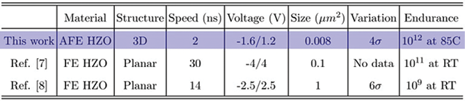
Paper #33.2, “FeRAM using Anti-ferroelectric Capacitors for High-speed and High-density Embedded Memory,” S. -C. Chang et al, Intel: a table benchmarking the FeRAM described in this paper with results previously reported for FeRAM devices with FE capacitors; it shows that FeRAM with scaled AFE HZO capacitors enables faster read/write operations with a lower voltage swing
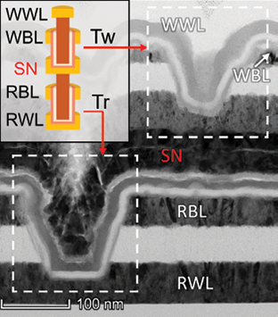
Paper #10.5, “Novel Vertical Channel-All-Around(CAA) IGZO FETs for 2T0C DRAM with High Density beyond 4F2 by Monolithic Stacking,” X, Duan/K. Huang et al, Chinese Academy of Sciences/Huawei: a TEM image of the vertically stacked 4F2 2T0C bit cell; the inset shows a schematic of the proposed 4F2 2T0C bit-cell, vertically connected to a read transistor’s gate
C. Power Devices
Toward a Better Understanding of SiC: Progress in silicon-carbide (SiC) material and device technologies has enabled mass production of 600–3,300 V SiC power MOSFETs and Schottky barrier diodes, which have led to substantial energy savings in various electric systems such as power supplies, photovoltaic inverters, air conditioners, electric vehicles, and railcars. Despite this progress, our basic understanding of the material properties and device physics of SiC is still somewhat lacking, making it difficult to develop guiding principles for designing SiC power devices. Also, the oxide/SiC interface remains extremely defect-rich, limiting the performance and reliability of SiC power MOSFETs. Researchers from Kyoto and Osaka Universities described in Paper #36.1 “Physics and Innovative Technologies in SiC Power Devices,” T. Kimoto et al, Kyoto University/Osaka University, several new insights and understandings in SiC power semiconductor technology, and presented a way to improve the SiC MOS interface for higher electron mobility through the use of a new process for gate-oxide formation.
GaN at Up to 10 kV: A Virginia Tech-led team described in Paper #5.5, a new power device concept they call a Multi-Channel Monolithic-Cascode high-electron-mobility transistor (MC2-HEMT). Made from AlGaN/GaN, the device monolithically integrates a low-voltage, enhancement-mode HEMT based on a single two-dimensional electron-gas (2DEG) channel, with a high-voltage, depletion-mode HEMT based on a stacked 2DEG multi-channel. It operates at a 10 kV breakdown voltage and has a specific on-resistance ∼2.5x smaller than SiC’s.
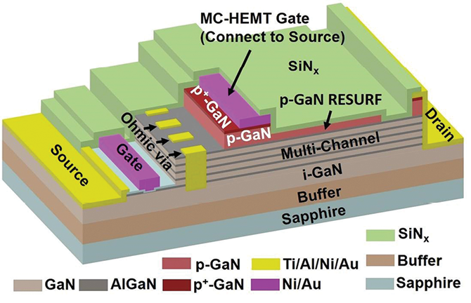
Paper #5.5, “Multi-Channel Monolithic-Cascode HEMT (MC2-HEMT): A New GaN Power Switch up to 10 kV,” M. Xiao et al, Virginia Polytechnic Institute/University of Southern California/Cambridge University/Enkris Semiconductors/Qorvo: a 3-D schematic of the AlGaN/GaN MC2-HEMT fabricated in this work. The SiNx passivation layer is partially removed to show the internal structure
Record Quantum Efficiency for NIR/SWIR Sensors: In Paper #23.4, STMicroelectronics researchers reported a 1.62 µm pixel-pitch global shutter sensor for imaging in the near-infrared (NIR) and shortwave infrared (SWIR) regions of the light spectrum. The sensor demonstrated record optical performance: an unprecedented quantum efficiency of >50% and a shutter efficiency of >99.94%. The breakthrough was made possible by use of a novel colloidal PbS quantum dot thin-film technology. The devices were fabricated on a 300 mm manufacturing toolset.
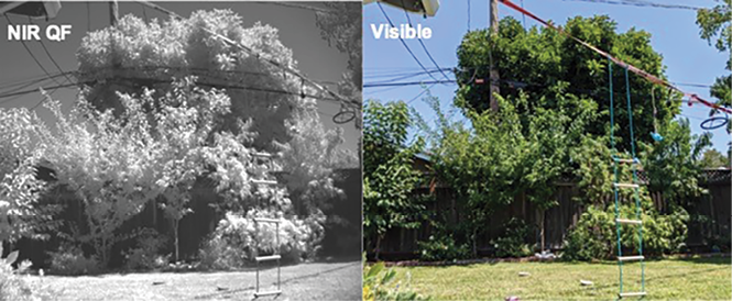
Paper #23.4, “1.62µm Global Shutter Quantum Dot Image Sensor Optimized for Near and Shortwave Infrared,” J.S. Steckel et al, STMicroelectronics: an outdoor image taken with the 940 nm NIR QF sensor (left) and with a high-end smartphone camera (right). The NIR image shows a significant difference in contrast, and the ability to clearly identify the black electrical wires hidden in the tree leaves, vs. the visible light image
3D Backside-Illuminated SPAD Imager Sensors: Unlike the CMOS image sensors found in smartphones, which measure the amount of light reaching a sensor’s pixels in a given timeframe, single photon avalanche diode (SPAD) image sensors detect each photon that reaches the pixel. Each photon is converted into an electric charge, and the electrons that result are eventually multiplied in avalanche fashion until they form an output signal. SPAD image sensors hold great promise for high-performance, low-light imaging applications, for depth sensing, and for fully digital system architectures. However, until now their performance has been limited by tradeoffs in pixel detection efficiency vs. pixel size, and by poor signal-to-noise ratios. Recently a charge-focusing approach was proposed to overcome these issues, but until now it has not been implemented. In late-news Paper #20.2, “3.2 Megapixel 3D-Stacked Charge Focusing SPAD for Low-Light Imaging and Depth Sensing,” K. Morimoto/J. Iwata et al, Canon, the researchers discussed how they did so, with the industry’s first 3D-stacked backside-illuminated (BSI) charge-focusing SPADs. The devices featured the largest array size ever reported for a SPAD image sensor (3.2 megapixels) and demonstrated a photon detection efficiency of 24.4%, and timing jitter below 100ps at 940 nm.
E. High-Frequency Electronics
Photonics Gives a Boost to mmW and THz Electronics: In coming years high-frequency electronics will be in the spotlight, as applications like 5G/6G communications strive to make use of ever-higher frequency bands (>100 GHz), and as fiber-optic and radio networks converge, making possible technologies like integrated radar/digital communications systems operating at 200–300 GHz. With an eye toward this future, researchers from Osaka University described in Paper #11.5 how they efficiently combined digital electronics with telecom-based photonic techniques for the generation/detection of millimeter-wave (mmW) and terahertz (THz) waves, to boost overall system performance. They conducted three different demonstrations to validate their approach: 1) a 15 Gb/s wireless link with optical fiber input @ 600 GHz; 2) real-time transmission of uncompressed 8-K UHD video at 48 Gb/s; and 3) a drone-mounted broadband mmW radar operating at 4 GHz–40 GHz.
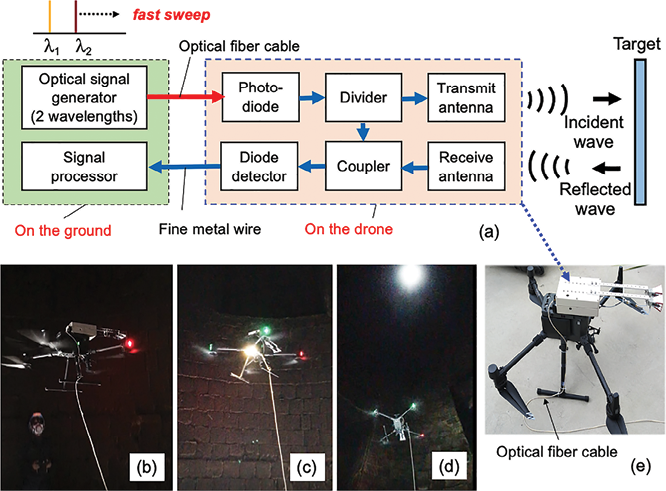
Paper #11.5, “Enabling Device Technologies for Photonics-Assisted Millimeter and Terahertz Wave Applications,” T. Nagatsuma et al, Osaka Univ.: (a) A block diagram of the ultra-broadband mmW radar mounted on a drone, (b-d) Photos of the drone flying in a chimney to inspect a wall, (e) Photo of the mmW radar mounted on a drone
F. Noteworthy Papers on Diverse Topics
A Stretchable Amplifier for Smart Textiles: A research team from Tsinghua University/Chinese Academy of Sciences/Cambridge University will described in Paper #16.4 stretchable all-inkjet-printed organic thin-film transistors and in-situ amplification circuits integrated in a strip-helix architecture. The organic devices are fabricated on plastic strips that are fashioned into a helix, which is then coiled around a stretchable fiber to be weaved or knitted into smart textiles. The helix-fiber design outperforms current state-of-the-art intrinsically stretchable devices, with ultralow power consumption of 681 pW, high subthreshold transconductance efficiency, and a high voltage gain of 214 V/V. The transistors and amplifier circuits demonstrated no significant changes in electrical performance up to a 50% extrinsic stretch.
Tailoring Ferroelectric Properties for Logic & Memory: Ferroelectric hafnium oxide, or hafnia, films are promising for advanced logic and memory devices because they are ultra-scalable, robust, CMOS-compatible and enable low-power designs. Their ferroelectric (FE) performance is dependent on their surface properties, and by modifying those properties (i.e., by functionalizing them) a film’s performance may be tailored to a specific application. However, there isn’t yet an atomic-level understanding of the relationship between a given surface functionalization and ferroelectric performance; most attempts to engineer FE performance by altering a hafnia film’s surface characteristics have been laborious trial-and-error efforts. In Paper #15.1 “Surface-Functionalized Hafnia with Bespoke Ferroelectric Properties for Memory and Logic Applications,” D.-H. Choe et al, Samsung, the researchers described the development of an automated algorithm for searching thermodynamically stable geometries of surface-functionalized FE HfO2. They used it to systematically investigate the surface functionalities of eight different hafnia crystal orientations, and how they impacted FE performance. They said, the technique is extendable to other oxide surfaces and functional groups, and will lead to precise control of hafnia’s FE properties for use in future devices.
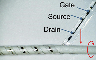
Paper #16.4, “High Stretchability Ultralow-Power All-Printed Thin-Film Transistor Amplifier on Strip-Helix-Fiber,” C. Jiang et al, Tsinghua University/Chinese Academy of Sciences/Cambridge University: a photo of the strip-helix-fiber OTFTs under coiling; red arrows indicate the directions that the strip and fiber move, respectively
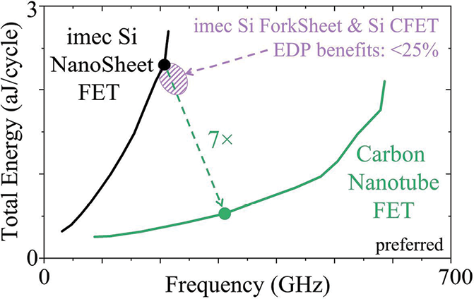
Paper #27.3, “Extended Scale Length Theory Targeting Low-Dimensional FETs for Carbon Nanotube FET Digital Logic Design-Technology Co-optimization,” C. Gilardi et al, Stanford University/Imec: pareto curves for energy vs. frequency for 15-stage inverter-based ring oscillators used in DTCO explorations
DTCO for Carbon Nanotube FETs: A Stanford/Imec team detailed in Paper #27.3 a design-technology co-optimization (DTCO) study on carbon nanotube FETs (CNFETs). At the device level, a new extended-scale-length theory that is crucial for low-dimensional FETs was developed, as well as a new CNFET leakage current compact model which includes inelastic band-to-band tunneling. Facilitated by these models, the team performed an in-depth DTCO analysis, which will enable CNFET technology to achieve a large energy delay product (EDP) benefit (a figure of merit for energy efficiency) versus advanced silicon technologies such as nano/forksheets and complementary FETs (CFETs) at the 2 nm node.
Luncheon—Tuesday, 14 December
Two eminent experts took part in the career-focused luncheon featuring industry and scientific leaders talking about their personal experiences in the context of career growth. The speakers were:
Dr. Vandebroek is a seasoned executive with extensive C-level experience at IBM, Xerox and UTC, and has served on public and private company boards since 2008. She is an expert in the creation and application of technologies that drive growth, and in the governance of inclusive and innovative global organizations. Dr. Vandebroek was previously VP of Emerging Technology Partnerships for IBM; Chief Operating Officer of IBM Research; CTO and Corporate Vice President at Xerox; and Board Chair of Xerox PARC, among other noteworthy roles.
Dr. Akinwande invented 2D memory, also known as atomristors. He has been honored with the 2018 Fulbright Specialist Award, 2017 Bessel-Humboldt Research Award, the U.S Presidential PECASE award by President Obama, the inaugural Gordon Moore Inventor Fellow award, the inaugural IEEE Nano Geim and Novoselov Graphene Prize, the IEEE “Early Career Award” in Nanotechnology, the NSF CAREER award, and several DoD Young Investigator awards, among many others.
Evening Panel Session—Tuesday evening, 14 December
A staple of the IEEE IEDM conference is the evening panel session, an interactive forum where experts give their views on important industry topics, and audience participation is encouraged to foster an open and vigorous exchange of ideas. The title of this year’s evening panel was “Is Hardware/Software Co-Design a Necessary Evil or a Symbiotic Partnership?” The panel was moderated by Myunghee Na, Semiconductor Technologist and VP of the Revolutionary Technology Center at SK hynix, it will explore the idea of what hardware/software co-design really means in terms of technology development and the introduction of new technology.
With this short report on the Evening Panel we conclude the wrap up of the 67th IEEE International Electron Devices Meeting.
Your comments are most welcome. Please write directly to the Editor-in-Chief of the Newsletter at daniel.tomaszewski@imif.lukasiewicz.gov.pl
2021 IEEE International Flexible Electronics Conference (IFETC-3)
The 2021 IEEE International Flexible Electronics Conference (IFETC-3) was held virtually on 9–12 August 2021, instead of downtown Columbus, Ohio. The meeting was intended as a hybrid format, but pivoted to fully virtual. IFETC-3 offered Sunday short courses, followed by 3-days of plenary & invited talks, interspersed amongst contributed talks. A minimal number of parallel sessions was used to maximize simulcast remote viewing. Recordings, including Q&A, were posted for registrants for 30-days following the meeting.
IFETC-3’s Technical Program covered a wide range of cutting-edge developments in printed and flexible electronics. IFETC, started in Ottawa, Canada (2018), focusing upon printed and flexible hybrid and non-hybrid materials, devices and systems. It will rotate between the Americas, Asia and Europe, heading to Qingdao, PRC in 2022. IFETC aims to bring together a wide variety of stakeholders, from chemists, materials scientists, physicists, to mechanical and electrical engineers, the fabrication and manufacturing communities, as well as end-users, e.g., packaging and medical communities. IFETC is where academia meets industry, and vice versa.
Just some key highlights included:
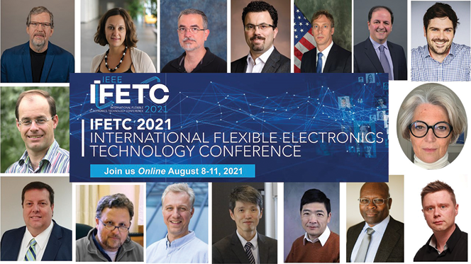
Figure 1. The 2021 IFETC conference committee represents a diverse group of international researchers, drawing new researchers into the IEEE EDS community
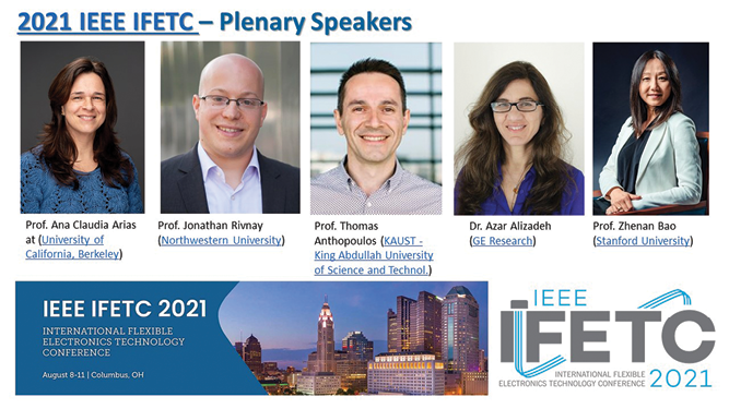
Figure 2. Medical wearables, advanced biosensors and printable manufacturing were prominently displayed within a slate of Plenary speakers, who represented well our potent WiE and young investigator communities
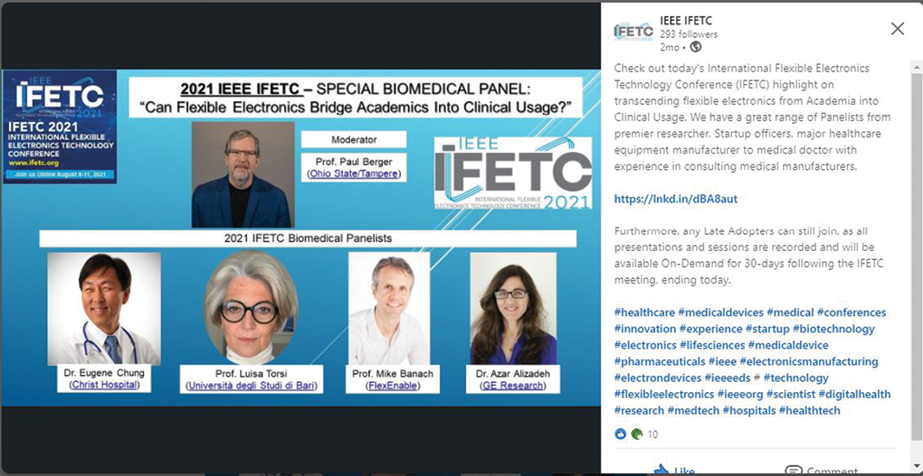
Figure 3. IFETC highlighted the transcendence of biomedical wearables from the academic research lab to the marketplace, tempered by prominent industrialists and leading medical doctors, who presented a sobering message of what is needed going forward
And IFETC-3 transcended the usual Zoom conference, thanks to Niels Benson (University of Duisburg—Essen), by implementing the Gather.town platform as a gathering place for socialization and technical discussions in between sessions. I witnessed at least one proposal brainstorming session between two investigators. And looking over the Columbus, Ohio skyline at the end of each day at the sky bar, sitting next to the crackling fire with a beverage of our choosing was spectacular! Cheers!
On behalf of the Conference, International Advisory and Steering Committees, we thank contributors to IFETC-3! Special thanks to the Organic Electronics Association (OE-A) for contributions to the short courses. I am pleased to inform you that IFETC is now present also on social media, i.e. LinkedIn: https://www.linkedin.com/company/ieee-ifetc and Twitter: https://twitter.com/IIfetc. Finally, IFETC is now branded too, with a new logo, and a dedicated webpage: www.ifetc.org for future years, like Qingdao, China in 2022.
Paul R. Berger
2021 General Chair
IEEE International Flexible Electronics Conference
https://ifetc.org
Highlights of IEEE EDTM2021
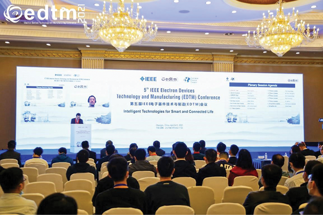
EDTM2021 Opening kicked-off both in-person and virtually
Sponsored by the IEEE Electron Devices Society (EDS), IEEE Electron Devices Technology and Manufacturing (EDTM) Conference is a premier conference providing a unique forum for discussions on a broad range of device/manufacturing-related topics. EDTM rotates among the hot-hubs of semiconductor manufacturing in Asia. EDTM2021 was successfully held in Chengdu, China, during 9–12 March 2021. Continuing its upward trend since EDTM was first launched in 2017, EDTM2021 was by all means another big success. The Theme for EDTM2021 was Intelligent Technologies for Smart and Connected Life. Due to the pandemic, EDTM2021 was held in hybrid formats including a large onsite/in-person gathering and a virtual conference. EDTM2021 was a four-day conference comprising a one-day tutorial/short course/workshop event on 9 March, and a three-day technical program including both oral and poster sessions. On Day-1, EDTM2021 was kicked off with two parallel tutorial tracks and four concurrent short course sessions. The two tutorial series focused on “Flexible electronics + Display” and “Future Communication and Computing”. The four short course sessions covered “Advanced Memories and Emerging Applications”, “Quantum Computing Technologies”, “Advanced Processing and Manufacturing” and “Ultra/Wide Bandgap Power Electronics”. Total twelve lectures were given by globally renowned experts. The highlight on 9 March also includes the “HIR Workshop Organizing Committee” organized by the IEEE Heterogeneous Integration Roadmap Committee and featured by eighteen experts from around the globe discussing the advances, challenges and future of HI technologies. EDTM2021 Technical Program started on 10 March with six Keynote Speakers talking about various hot topics, including Dr. Haijun Zhao (Co-CEO of SMIC) on “Creating Values through Innovations on Mature Nodes of Technologies of Integrated Circuits”, Prof. Xiang Zhang (President, University of Hong Kong) on “How to build a camera with highest resolution: a photonics perspective”, Mr. Teruo Hirayama (Executive Chief Engineer, Sony Corp.) on “The power of image sensors for innovation”, Prof. Arokia Nathan (University of Cambridge) on “Thin Film Transistor Architectures for Advanced Analog Signal Processing”, Prof. Ru Huang (Vice President, Peking University) on “Ferroelectric-based device: revived as a low-power technology booster for diverse applications”, and Dr. Jeff Xu (Director, HiSilicon Research) on “Ubiquitous Computing Drives Future Semiconductor Technology”. The Plenary was closed with a Closing Banquet Speech given by Prof. Ilesanmi Adesida (Provost, Nazabaryev University) entitled “The Development of an International Research University in the Big Steppe of Kazakhstan”. EDTM2021 Technical Program core contains about 289 technical papers accepted after vigorous peer reviewing, including 172 oral (organized into 36 Sessions) and 117 interactive presentations. EDTM2021 had a total registered attendance of 800+, including 492 for the Technical Program (283 in-person and 209 virtual), 156 for Tutorials and 158 for Short Courses. EDTM2021 also featured a “Young Engineers’ Networking” event and a “Women-in-Engineering Summit”. EDTM2021 concluded with the Closing Banquet, a tradition of EDTM, full of Sichuan gourmet food, fun, and tears. EDTM2022 will move to Oita, Japan during 6–9 March 2022.
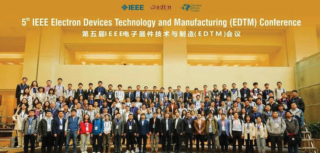
Participants of 5th IEEE EDTM Conference attending an in-person mode
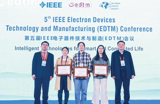
(From Left) Prof. Tiancun Ye (General co-Chair, 5th) and Prof. Huaqiang Wu (TPC Chair, 1st) presented the Best Student Paper Awards: First Place Award—Nianying Wang (3rd from left; paper: N. Wang, et al., Shanghai Inst. Microsystem and Information Technology, CAS, ShanghaiTech University, University of CAS—“Double-Deck Metal Solenoids 3D Integrated in Silicon Wafer for Kinetic Energy Harvester”); Third Place Award—Qiumeng Wei (2nd from left; paper: Q. Wei, et al., Inst. Microelectronics, Tsinghua University, Beijing Innovation Center for Future Chips, Tsinghua University—“Double-Deck Metal Solenoids 3D Integrated in Silicon Wafer for Kinetic Energy Harvester”); and Second Place Award—Shunjie Yu (4th from left; paper: S. Yu, et al., University of Science and Technology of China, Shandong University—“β-Ga2O3 Micro-Flake FET SBPD with Record Detectivity of 3.87×10¹⁷ Jones for Weak Light Detection”)
Albert Wang
2021 General Chair
University of California, Riverside, USA
Tianchun Ye
2021 General Co-Chair
Institute of Microelectronics, CAS, China
Huaqiang Wu
2021 Technical Program Chair
Tsinghua University, China
Subramanian Iyer
2021 Technical Program Co-Chai
University of California, Los Angeles, USA
2021 IEEE International Interconnect Technology Conference (IITC)
The International Interconnect Technology Conference (IITC), sponsored by the IEEE Electron Devices Society and co-sponsored by the Japan Society of Applied Physics, is the premier conference on interconnect technology, featuring cutting-edge research in the areas of advanced metallization and 3D integration for ULSI applications.
The 24th IITC was held on 6–9 July 2021 in a hybrid format of virtual and face-to-face meetings (Kyoto Research Park, Kyoto, Japan). Pre-recorded presentations were live-streamed and Q&A sessions were also held live.
The IITC 2021 live sessions were attended by 348 people from 14 different regions (Figure 1). Due to COVID-19, the number of guests who came to the conference room was limited (∼10). The technical program included 2 plenary lectures, 12 invited lectures, 27 oral presentations, and 25 posters, presenting original and state-of-the-art research. On-demand videos were available until 31 August 2021.
Workshop Program
Prior to the technical program, a workshop entitled “Metallization Technologies and Their Applications in IoT and AI Devices” was held on 6 July, featuring seven leading experts.
M. Tsujimura (Ebara) reported on Digital and Green Transformation, which are driving the semiconductor market, and the revolution in manufacturing equipment. Experts in different technical fields discussed the most advanced key technologies for current and future applications of IoT and AI devices: 3D Flash memory by M. Tagami (KIOXIA), STT-MRAM by K. Lee (Samsung), Back-Illuminated-CIS by Y. Kagawa (Sony Semiconductor Solutions), Nano bridge Technology by M. Tada (NanoBridge Semiconductor), Reliability challenges in advanced interconnects by O. V. Pedreira (IMEC), and Si photonics by B. J. Offrein (IBM).
Technical Program
The technical program started with an opening speech by General Chair K. Ueno of Shibaura Institute of Technology, followed by the IITC2020 award ceremony.
Michel Lerme Best Paper Award was given to K. Motoyama, IBM Research for the work “Co-doped Ru liners for highly reliable Cu interconnects with selective Co cap”.
LAM Research Best Student Paper Award was given to Y. Yamada, Tohoku University for the work “Thermodynamic Exploration of Co–Alloy Diffusion Barriers for Advanced Cu Interconnect”.
Best Poster Award was given to T. Kuge, Tohoku University for the work “The structural origin of the minimum diffusion barrier thickness of ultra-thin TaNx”.
After the ceremony, two keynotes were given by the technology leaders:
Among the topics discussed during the Conference it is worthwhile to mention “Old New” materials and process steps that were previously used in the Si front-end processes. E.g. molybdenum (Mo) was presented as the “new” contact or wiring material, and dry etching was discussed as the “new” interconnect formation method instead of the damascene process. In addition, various applications of selective deposition processes such as “old” tungsten chemical vapor deposition (W-CVD) and Self-Assembled Monolayer (SAM) were explored to overcome the scaling issues. It becomes noticeable that apart from miniaturization, the “old” approaches really work for the “new” challenges. As for the technology node, 7 nm–5 nm node process for production and <=3 nm node process for R&D were discussed. Furthermore, the potential of 3D heterogeneous integration technology to realize any future integration of circuits, devices, and systems was also discussed.
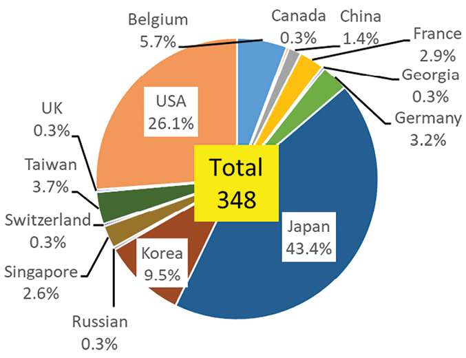
Figure 1. Percentage of participants from each country
The following papers are examples of presentations that received a lot of attention from the participants:
| CATEGORY | TITLE | SPEAKERS |
| Advanced Interconnect | Advanced interconnect challenges beyond 5nm and possible solutions | Kichul Park (Samsung) |
| EM performance improvements for Cu interconnects with Ru-based liner and Co cap in advanced nodes | Koichi Motoyama (IBM) | |
| Integration/pattering | EUV patterning considerations for BEOL scaling | Nilson Felix (IBM) |
| Analysis of edge placement error (EPE) at the 5 nm node and beyond | Robert Socha (ASML) | |
| RC Scaling | On-die interconnect technologies for future technology nodes | Mauro Kobrinsky (Intel) |
| MOL Contacts | Contact module progress and challenges in advanced CMOS technologies | Nicolas Breil (AMAT) |
| Reliability | Reliability Characterization on Advanced FinFET Technology | Kihyun Choi (Samsung) |
| 3D | Opportunities and challenges brought by 3D-sequential integration | Perrine Batude (CEA-Leti) |
| Memory | Enabling Ferroelectric Memories in BEOL—towards advanced neuromorphic computing architectures | David Lehninger (Fraunhofer) |
| Commercialization of MRAM—Historical and Future perspective | Sumio Ikegawa (Everspin) | |
| Novel System | Resistive memories for neuromorphic hardware | Elisa Vianello (CEA-Leti) |
| Beyond Cu | Intermetallic compounds for Interconnect metal beyond 3 nm node | Junichi Koike (Tohoku Univ.) |
Invited Speakers
The Virtual 2021 IITC had some new activities. One of them was an exhibitor session from 7–9 July in between the technical sessions, where exhibitors gave presentations and virtual booth tours. The second new activity was the poster session, which consisted of five-minute presentations. Each of them was followed by an interview with the individual author in a separate virtual room to discuss the presented work with the audience. The third new activity was a networking reception where participants could converse with each other in close proximity on a virtual platform, creating an atmosphere similar to an actual social gathering.
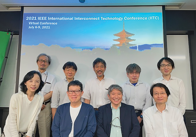
Members of on-line conference support group in Kyoto
This new format was proposed and implemented by Semiconductor Portal Inc. (Japan), the operator of this year’s and 2013’s IITC, and was well received. In the future, it will be necessary to run conferences in such a way that participants feel as if they were attending an actual conference. 2021 IITC was one of the great examples of this approach.
The next IITC will be held on 27–30 June, 2022 at Holiday Inn San Jose, California, USA. Looking forward to seeing you all there.
Susumu Matsumoto
Tower Partners Semiconductor
Shinichi Ogawa
AIST
Review of the 2021 IRPS
The IEEE International Physics Reliability Symposium (IRPS) has been the premiere conference for engineers and scientists to present new and original work in the area of microelectronics reliability for 60 years. Drawing participants from the Americas, Europe, Asia, and all other parts of the world, IRPS seeks to understand the reliability of semiconductor devices, integrated circuits, and microelectronic systems through an improved understanding of both the physics of failure as well as the application environment.
The 2021 IRPS was held in a virtual format starting on 21 March and running until 24 March 2021—the duration of which the recorded presentations were accessible to the registrants. The virtual event was attended by almost 500 registered participants, which was 25% higher than the previous year and a record for recent years.
The highlights of the 2021 technical program include:
The conference encompassed a wide range of topics, ranging from Circuit Reliability and Aging, Emerging Memory Reliability, ESD and Latchup, Failure Analysis, Gate/MOL Dielectrics, IC Product Reliability, Memory Reliability, Metallization/BEOL Reliability, Neuromorphic Computing Reliability, Packaging and 2.5/3D Assembly, Process Integration, Reliability Testing, RF/mmW/5G Reliability, Soft Error, System Electronics Reliability, Transistor Reliability, to Wide-Bandgap Semiconductors- GaN and SiC. The 2021 Special focus topics were Circuit Reliability and Aging (EDA Tools, Sensors, and Aging Aware Designs), Wide Bandgap Devices (with emphasis on Reliability, Availability and Serviceability (RAS), self-healing, aging aware design, design tools), Emerging Memory / Reliability issues of Neuromorphic Computing (PCM, MRAM, RRAM, ferroelectrics), and Reliability of RF/mmW/5G Devices (CMOS, SiGe BiCMOS, SOI, GaAs, GaN).
The conference formally kicked off on 21 March 2021, with a welcome address by the General Chair Robert Kaplar, Sandia National Labs, and an overview of the technical program by the Technical Program Chair Chris Connor, Intel. Each day started with a plenary keynote by industry executives listed below.
This year, tutorials and technical sessions were offered in parallel which gave the attendees greater flexibility to not only to listen to focused lectures from domain experts but also to learn about the latest research discoveries throughout the entire 4 day conference. Tutorials were given by instructors who are authorities in their respective reliability fields—either veteran IRPS presenters for established topics or invited specialists in emerging topics. A total of 22 tutorials were offered on topics ranging from 3D integration, 5G/mmW/RF, GaN, memory reliability, automotive, advanced interconnect, cryogenic electronics, design automation, ESD, to FinFET self-heating.
Day 1 ended with three Year-In-Review (YIR) talks, a segment always appreciated by IRPS attendees, allowing them to quickly catch up on recent developments in multiple areas. In this year’s Year-in-Review (YIR) several speakers covered the past year of literature on (YIR1) FinFET versus Gate-All-Around FET Reliability, (YIR2) Considerations for Physics-Based Reliability Testing Development, and (YIR3) Industry Council on ESD Target Levels: Review of Achievements, Activities, and Initiatives.
Technical session presentations consisted of 107 Oral (of which 20 were invited) and 53 Poster papers, previously selected by 18 subcommittees. Due to the virtual nature of the conference, the papers were typically presented as prerecorded video clips which resulted in higher quality presentations. Poster presenters were allotted limited time to introduce their work and, to emulate the poster session experience, they could discuss their work with interested audience members in separate video calls. Workshops were held on Day 3 where attendees enjoyed informal discussions on specific reliability topics with the guidance of experienced moderators. As an added perk for this year’s attendees, all recorded talks were available after the conference.
The IRPS subcommittees highlighted the following contributed papers:
After the conference, the following awards were announced:
Best Paper
Correlation Between MOSFETs Breakdown and 4HSiC Epitaxial Defects
P. Fiorenza, S. Adamo, M. S. Alessandrino, C. Bottari, B. Carbone, C. Di Martino, A. Russo, M. Saggio, C. Venuto, E. Vitanza, E. Zanetti, F. Giannazzo and F. Roccaforte Consiglio Nazionale delle Ricerche—Istituto per la Microelettronica e Microsistemi (CNR-IMM) and STMicroelectronics, Catania, Italy.
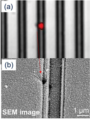
(a) Emission microscopy of the wafer level test of a defective device; (b) SEM image shows the presence of a pipe on the whole metalization
Best Student Paper
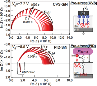
Assessment of plasma damaged SiN by TDIS: Nyquist plots of SiN after (top) electrical stress or (bottom) Ar plasma exposure
Tomohiro Kuyama, Keiichiro Urabe, Koji Eriguchi, Kyoto University, Kyoto, Japan
Best Posters
BTI Arbitrary Stress Patterns Characterization & Machine-Learning Optimized CET Maps Simulations
L. Gerrer, J. Cluzel, F. Gaillard, X. Garros, X. Federspiel, F. Cacho, D. Roy, and E. Vincent
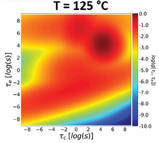
Capture/emission times (CET) map of the threshold voltage shift due to BTI for temperature 125 °C obtained using the genetic algorithm applied for the BTI model
CEA-LETI Grenoble, France and ST Microelectronics, Crolles, France
Mitigating Switching Variability in Carbon Nanotube Memristors
J. Farmer, W. Whitehead, A. Hall, D. Veksler, G. Bersuker, D. Gao, Al-Moatasem El-Sayed, T. Durrant, A. Shluger, T. Rueckes, L. Cleveland, H. Luan, R. Sen
Measurements of Set and Reset currents during 5 ns repeated switching process
The Aerospace Corporation, Los Angeles, CA, USA, Nanolayers Research Computing LTD, London, UK, Nantero Inc., Oburn, MA, USA
People’s Choice
Off-state TDDB in FinFET Technology and its Implication for Safe Operating Area
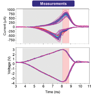
M. Toledano-Luque, P. Paliwoda, M. Nour, T. Kauerauf, B. Min, G. Bossu, M. Siddabathula, T. Nigam
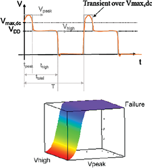
A standard three V-level waveform considered for the analysis (top); Failure rate for FEOL TDDB as a function of Vhigh and Vpeak with Vpeak > Vhigh at fixed tpeak and thigh
GlobalFoundries, Malta, NY, USA, Dresden, Germany, Santa Clara, CA, USA
TDDB Reliability in Gate-All-Around Nanosheet
Huimei Zhou, Miaomiao Wang, Ruqiang Bao, Tian Shen, Ernest Wu, Richard Southwick, Jingyun Zhang, Veeraraghavan Basker, Dechao Guo,
IBM, Albany, NY, USA
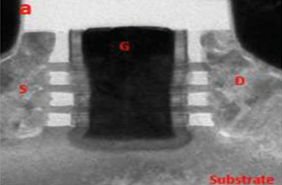
TEM image of a stacked GAA NS transistor
Next year, IRPS 2022 will return to an in person format from 27–31 March 2022, in Dallas, Texas. The latest information can be found on https://www.irps.org/.
Chris Kim
IRPS 2022 Publicity Chair
University of Minnesota