Technical Briefs
2023 IEEE International
Electron Devices Meeting
Highlighted Advances in Critical
Semiconductor Technologies
with the Theme “Devices for a
Smart World Built Upon
60 Years of CMOS”
Since it began in 1955, the IEEE International Electron Devices Meeting (IEDM) has been where the world’s best and brightest electronics technologists go to learn about the latest breakthroughs in semiconductor and related technologies. That tradition continued last year, when the 69th annual IEEE IEDM conference took place in-person on 9-13 December 2023 at the Hilton San Francisco Union Square hotel, with online access to recorded content available afterward.
The 2023 IEDM technical program, supporting the theme, “Devices for a Smart World Built Upon 60 Years of CMOS,” consisted of more than 225 presentations plus a full slate of panels, Focus Sessions, Tutorials, Short Courses, a career luncheon, supplier exhibit, and IEEE/EDS award presentations.
“The IEDM offers valuable insights into where the industry is headed because the leading-edge work presented at the conference showcases major trends and paradigm shifts in key semiconductor technologies,” said Jungwoo Joh, IEDM 2023 Publicity Chair and Process Development Manager at Texas Instruments. He continued: “For example, this year many papers discuss ways to stack devices in 3D configurations. This is of course not new, but two things are especially noteworthy about this work. One is that it isn’t just happening with conventional logic and memory devices but with sensors, power, neuromorphic, and other devices as well. Also, many papers don’t describe futuristic laboratory studies, but rather specific hardware demonstrations that have generated solid results, opening pathways to commercial feasibility.” “Finding the right materials and device configurations to develop transistors that will perform well with acceptable levels of reliability remains a key challenge,” said Kang-ill Seo, IEDM 2023 Publicity Vice Chair and Vice President, Semiconductor R&D, Samsung Semiconductor. He added: “This year’s program shows that electrothermal considerations remain a key focus, particularly with attempts to add functionality to a chip’s interconnect, or wiring, which is fabricated using low-temperature processes.”
Here are details of the 2023 IEEE International Electron Devices Meeting:
Tutorial Sessions
On Saturday, 9 December, six Tutorial sessions on emerging technologies were presented by experts in the field to bridge the gap between textbook-level knowledge and leading-edge current research, and to introduce attendees to new fields of interest. The tutorials are listed below together with a brief description of their content:
Short Courses
On the next day of the IEDM, Sunday, 10 December, two full-day Short Courses were held in parallel. In contrast to the Tutorials, they were focused on a single technical topic. They offered the opportunity to learn about important areas and developments, and to network with global experts. The Short Courses and their content are presented below:
Welcome and Awards
The main part of the 2023 IEDM started on Monday, 11 December with the Welcome by Dina Triyoso, General Chair of the Conference. Afterwards, recipients of the following awards were announced:
Technical Program
The technical program of 2023 IEDM consisted of 41 technical sessions including one Plenary Session held on Monday immediately after the Welcome and Awards ceremonies and four Focus Sessions.
During the Plenary Session, three Plenary Presentations were given:
Below, we briefly report four Focus Sessions devoted to key emerging technologies. We describe their leading themes and content.
Neuromorphic Computing for Smart Sensors (Session #7)—Interest is growing in neuromorphic computing, where electronic devices and systems are designed to emulate how the brain works. The hope is that this will make possible new and better solutions to difficult computing challenges. This Focus Session contained invited papers describing recent advances in neuromorphic computing and smart sensors:
Logic, Memory, Package and System Technologies for Future Generative AI (Session #15)—Generative artificial intelligence (AI) has been all the buzz lately, with its potential to increase productivity and efficiency in many spheres of human endeavor. However, creating the logic, memory and other devices needed for future generative AI systems is a formidable technical challenge. This Focus Session covered system requirements, technical barriers, and solutions for AI computing and included the papers:
3D Stacking for Next-Generation Logic & Memory by Wafer Bonding and Related Technologies (Session #19)—As the feature sizes in leading-edge CMOS devices approach atomic dimensions, traditional scaling has become much more difficult and expensive. One way to meet the demands of ever-growing computing and AI workloads, while still achieving the traditional PPAC benefits of scaling (performance, power, area, and cost), is to stack integrated circuits vertically, in 3D configurations. The following works were presented during this Focus Session:
Sustainability in Semiconductor Device Technology and Manufacturing (Session #28)—This Focus Session was about sustainability in device technology and manufacturing because it has never been more important to use Earth’s finite resources more efficiently and to reduce associated environmental impacts. Six papers were presented at this Focus Session:
The following sections present summaries of the most noteworthy, in our opinion, papers presented during the technical sessions of the 2023 IEDM. Several papers can be assigned to common thematic groups. We present these groups first. Then, we present other noteworthy papers on diverse topics.
CMOS Scaling: CFETs and 2D Channel FETs
Nanosheet-based transistors, and 3D complementary FETs (CFETs) built from nanosheets, are key to continuing Moore’s Law scaling. Nanosheets are gate-all-around (GAA) transistor architectures where stacks of silicon channels are completely surrounded by the gate. They offer better electrostatic control than FinFETs, relatively high drive currents, and variable widths. CFET architectures are highly integrated 3D designs where n-FET and p-FET nanosheets are stacked on top of one other. These stacked devices may be built monolithically (on one wafer), or sequentially (built on separate wafers and then transferred and integrated). At the IEDM, a number of papers advanced the state-of-the-art in these areas. Among them, there were papers from TSMC and Intel that discussed ways to scale silicon (Si) CMOS technology in the nearer term.
A Practical, Monolithic CFET Architecture: In the late-news paper #29.6, “Complementary Field-Effect Transistor (CFET) Demonstration at 48nm Gate Pitch for Future Logic Technology Scaling”, TSMC researchers unveiled what they call a practical, monolithic CFET architectural approach for logic technology scaling. It features 48nm-gate-pitch stacked n-FET-on-p-FET silicon nanosheet transistors (Fig.1). These demonstrated high on-state current/low subthreshold leakage, leading to an impressive on/off current ratio (six orders of magnitude). They also exhibited a relatively high yield, with a FET survival rate of >90%. Although previous work has shown that functional CFET devices can be built on 300mm wafers, the gate pitches of those devices have been too large for future scaling. In this work, a more relevant 48nm gate pitch was achieved with a vertically stacked n/p source-drain (SD) epitaxy, comprising middle dielectric isolation, an inner spacer, and n/p SD isolation. While other essential features still must be integrated to unleash CFET technology’s potential, this work paves the way for that to happen.
Figure 1. Inline cross-section TEM demonstration of a monolithic CFET with a gate pitch of 48nm and with nFETs placed above pFETs, and both types of transistors surrounded by a single metal Gate (Paper #29.6, “Complementary Field-Effect Transistor (CFET) Demonstration at 48nm Gate Pitch for Future Logic Technology Scaling,” S. Liao, et al, TSMC).
A CFET-Based CMOS Inverter: Intel researchers presented in the paper #29.2, “Demonstration of a Stacked CMOS Inverter at 60nm Gate Pitch with Power Via and Direct Backside Device Contacts,” a 3D monolithic CFET device they built, consisting of 3 n-FET nanoribbons on top of 3 p-FET nanoribbons, with 30 nm of vertical separation between them (Fig. 2). In an industry first, they used this device to build fully functional inverters (test circuits) at a 60nm gate pitch. The devices also featured vertically stacked dual-S/D epitaxy; dual metal work function gate stacks connecting the n- and p- transistors; and integration with backside power delivery and direct backside device contacts. The researchers also described a nanoribbon “depopulation” process, for which unequal numbers of n-MOS/p-MOS devices are needed. The work helps to increase understanding of the potential to scale CFETs for logic and SRAM applications and to understand key process enablers.
Figure 2. a) TEM micrograph of the CFET device following vertically stacked dual source-drain (SD) epitaxy at contacted poly pitch (CPP) = 60 nm, b) the inverter voltage transfer curve, which verifies that all components make a well-balanced inverter (Paper #29.2, “Demonstration of a Stacked CMOS Inverter at 60nm Gate Pitch with Power Via and Direct Backside Device Contacts,” M. Radosavljevic´, et al, Intel).
Record Results from Stacked NMOS Nanosheets with TMD Channels: Research on scaling of devices in the beyond-CMOS domain was presented in paper #2.1 “Monolayer-MoS2 Stacked Nanosheet Channel with C-type Metal Contact”. Currently, nanosheet scaling is accomplished by thinning the Si channels, but work is ongoing to find practical ways to use ultra-thin transition metal dichalcogenides (TMDs) as the channel material instead. TMDs such as MoS2 are called monolayer/2D materials because they’re just an atomic layer thick. A TSMC-led team discussed the unprecedented performance of two stacked NMOS nanosheets with MoS2 channels (Fig.3). The 40nm gate-length NMOS devices exhibited positive threshold voltage (VTH ∼1.0 V); high on-current (ION ∼370 µA/µm at VDS = 1 V); a large on/off ratio (108); and low contact resistance (RC ∼0.37-0.58 kΩ-µm). Key to these results was a novel C-shaped wrap-around contact offering greater contact area and gate stack optimization. The devices exhibited acceptable mechanical stability but the researchers said more research is needed to mitigate defect creation in the MoS2 channels.
First True 2D CMOS Demonstration: Another interesting work on scaling of beyond-CMOS devices was presented in paper #10.1 “Status and Performance of Integration Modules Toward Scaled CMOS with Transition Metal Dichalcogenide Channel.” FET devices of each polarity (n-FETs and p-FETs) must offer matched performance for proper operation for CMOS logic. But while MoS2 is a suitable TMD material for n-type devices, it doesn’t work well for p-type devices, where the TMD material WSe2 is better suited. Also, both extremely thin materials must be robust enough to withstand typical fabrication processes. In the industry first, a TSMC-led team described the well-matched n- and p-MOS transistors made using these two TMD channel materials, respectively (Fig.4). The robustness of these highly scaled (∼50nm channel lengths) and high current-density materials was demonstrated by growing them separately on sapphire and then transferring them die-by-die to a 300 mm silicon wafer to integrate them. The devices showed nearly unaltered performance after this transfer process, with a high output current (∼410 µA/µm) at the same gate overdrive for both n- and p-FETs (VDS = 1 V). In addition, p-FET mobility reached a record high level (∼30 cm2 /V∙s).
Figure 3. Dark-field TEM image of the stacked 1L-MoS2 channel structure with a C-type metal contact (Paper #2.1, “Monolayer-MoS2 Stacked Nanosheet Channel with C-type Metal Contact,” Y-Y Chung, et al, TSMC/Nat’l Yang Ming Chiao Tung Univ./National Applied Research Laboratories).
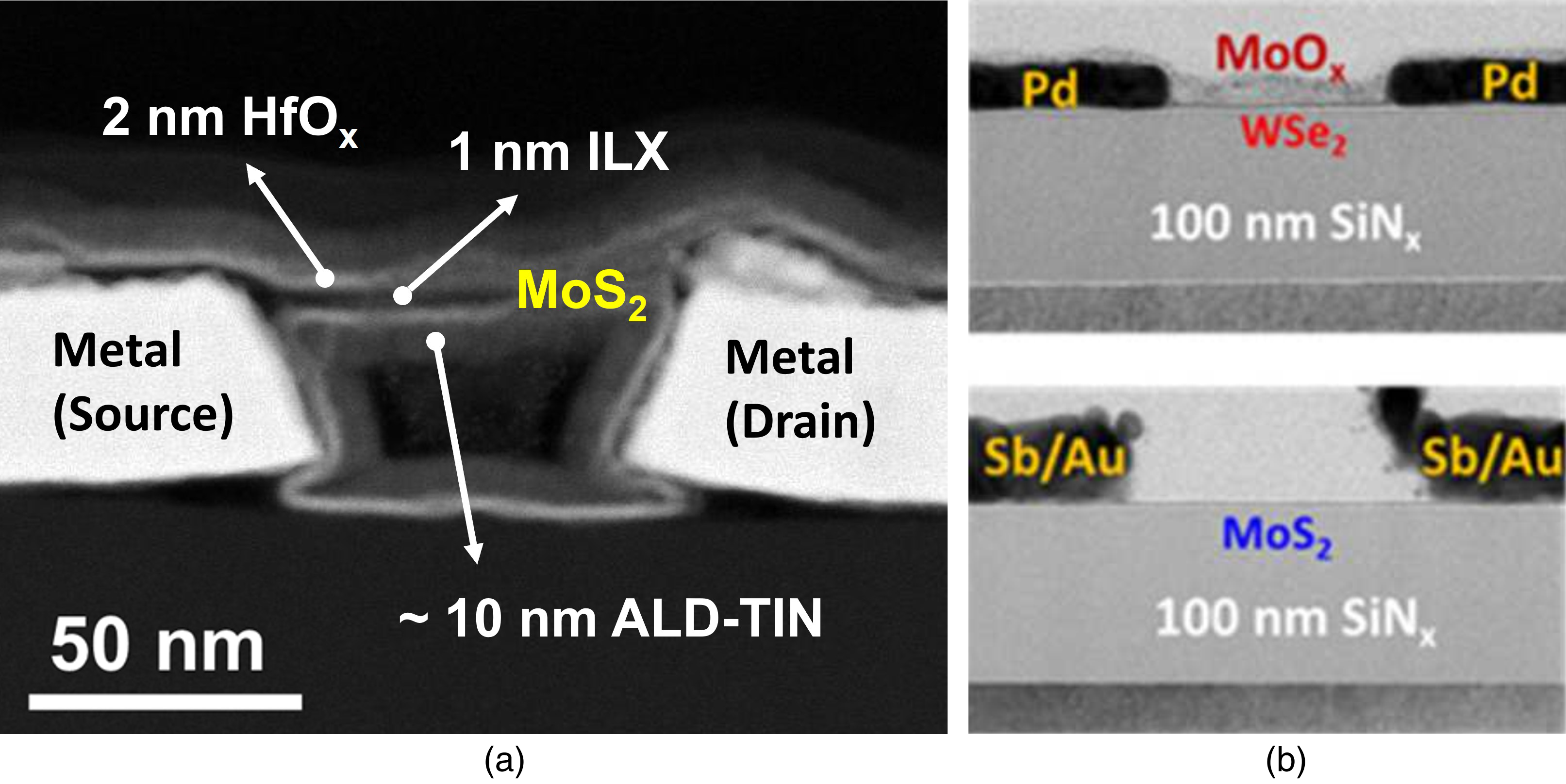
Figure 4. A cross-sectional TEM of the suspended MoS2 nanosheet structure with conformal gate stack comprising 10nm TiN, 2nm HfOx, and 1 nm ILX (interfacial dielectric); b) cross-sectional TEM images of integrated n/p FETs (Paper #10.1, “Status and Performance of Integration Modules Toward Scaled CMOS with Transition Metal Dichalcogenide Channel,” A-S Chou, et al, TSMC/Nat’l Taiwan Univ/Nat’l Yang Ming Chiao Tung Univ.)
Memories
Dense, Fast, Low-Voltage, High-Endurance STT-MRAM: Non-volatile memories retain data when power is shut off, making them useful in embedded applications such as automotive. Flash memory has been the go-to choice for embedded, but is falling short at advanced nodes. Non-volatile magnetic memory (Magnetoresistive RAM, or MRAM) stores data as a magnetic state, not as an electrical charge, and has made inroads into embedded applications. A type called Spin-Transfer Torque MRAM (STT-MRAM) offers fast write speeds, the potential for very high density, low-power operation, and long endurance. In paper #21.5, “Low Voltage (<1.8V) and High Endurance (>1 M) 1-Selector/1-STT-MRAM with Ultra-Low (1 ppb) Read Disturb for High Density Embedded Memory Arrays”, a TSMC-led team described the STT-MRAM with a 1S1R (1 selector/1 resistor) crosspoint array architecture, having more than twice the density (>2.2x) of conventional 1T1R (1 transistor/1 resistor) designs at a 16 nm technology node (Fig. 5). What makes this possible is the use of a specially engineered selector material, SiNGeCTe. The STT-MRAM demonstrated low-voltage operation (<1.8 V); high-speed switching (off-on/on-off transitions of 2.5 ns/3 ns, respectively); and outstanding read/write endurance (>1e9/>1e6 cycles, respectively). The architecture is said to be suitable for stackable 3D memory arrays.
A New Way to Scale DRAMs: DRAM is the workhorse memory of electronic systems, but scaling it to 10 nm and below brings difficult challenges. At advanced nodes, patterning the extremely small features of conventional 6F2 buried cell array transistors is extremely difficult, as is suppressing “row hammer” electrical interference from nearby cells. However, Samsung researchers saw an opportunity to scale DRAM further with vertical-channel transistors (VCTs) using IGZO (indium gallium zinc oxide) as the channel material. IGZO offers high electron mobility, low leakage, and a high on/off ratio that leads to low power consumption and is suitable for low-temperature processing. In paper #6.3, “Highly Manufacturable, Cost-Effective, and Monolithically Stackable 4F2 Single-Gated IGZO Vertical Channel Transistor (VCT) for sub-10 nm DRAM,” they detailed the first successful integration of a 4F2 single-gated IGZO-VCT, monolithically stacked on top of core/peripheral transistors with no need for wafer bonding (Fig. 6). They said the devices are suitable for sub-10 nm DRAMs. They demonstrate low leakage current (IOFF <1 fA/cell); subthreshold swing (SS) of 164 mV/dec, and adequate threshold voltage (VT = -1.73 V at 85 ˚C). The vertical architecture also can fully suppress “row hammer” interference, because the active region isn’t shared with adjacent cells.
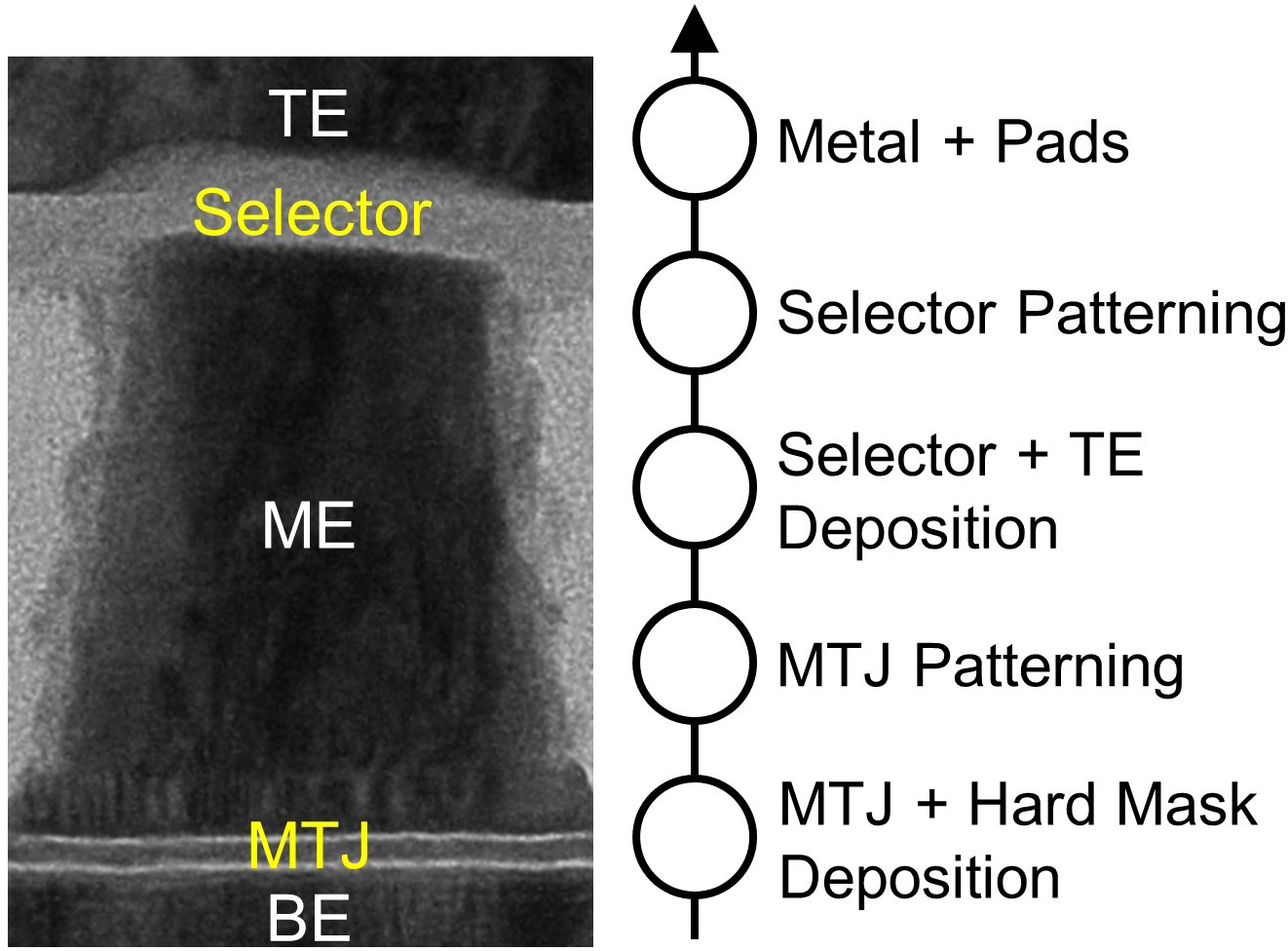
Figure 5. A TEM image of the integrated 1S1R STT-MRAM memory (Paper #21.5, “Low Voltage (<1.8 V) and High Endurance (>1 M) 1-Selector/1-STT-MRAM with Ultra-Low (1 ppb) Read Disturb for High Density Embedded Memory Arrays,” E. Ambrosi, et al, TSMC/Taiwan Semiconductor Research Institute).
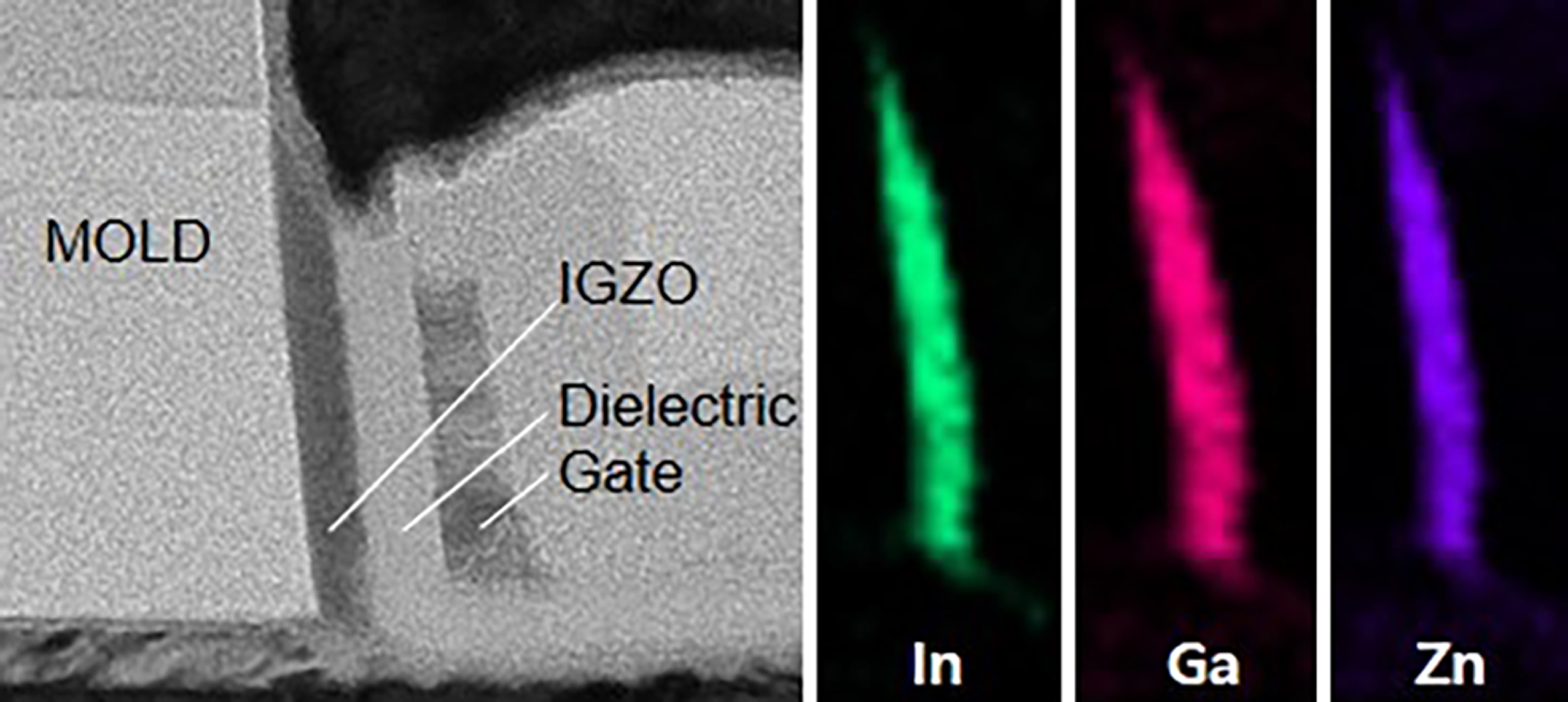
Figure 6. X-TEM image (left) and EDS analyses (right) of the single-gated IGZO vertical channel transistor after gate stack formation.(Paper #6.3, “Highly Manufacturable, Cost-Effective, and Monolithically Stackable 4F2 Single-Gated IGZO Vertical Channel Transistor (VCT) for sub-10nm DRAM,” D. Ha, et al, Samsung).
Non-Volatile Ferroelectric w/DRAM-Like Performance, for AI & Machine Learning: Rapid growth in the size of the data models used in artificial intelligence (AI) and machine-learning (ML) applications is creating an urgent need for higher-bandwidth memory solutions. While new compute paradigms like near-memory-compute and processing-in-memory are being investigated, the best near-term opportunity is to outfit existing, traditional computing architectures with more efficient memory for faster data movement and to accommodate larger models. In paper #15.7, “NVDRAM: A 32Gb Dual Layer 3D Stacked Non-Volatile Ferroelectric Memory with Near-DRAM Performance for Demanding AI Workloads,” presented during the Focus Session “Logic, Memory, Package and System Technologies for Future Generative AI” (see above), Micron researchers unveiled a memory technology for these uses which they call NVDRAM (Fig. 7). It is the world’s first dual-layer, high-performance, high-density (32Gb), stackable and nonvolatile ferroelectric memory technology. It combines the non-volatile, high-endurance nature of ferroelectric memory cells with DRAM-like read/write speeds and endurance, and also surpasses the retention performance of NAND memory. NVDRAM uses an ultra-scaled (5.7 nm) ferroelectric capacitor as the memory cell, and a dual-gated, stackable, polycrystalline silicon transistor as the access device. To achieve high memory density, two memory layers are fabricated above CMOS circuitry in a 48 nm pitch, 4F2 architecture. Full package yield is demonstrated from −40 °C to 95 °C, along with reliability of 10 years (for both endurance and retention).
A Larger Memory Window for 3D NAND: Non-volatile 3D NAND flash memory is widely used for data storage in enterprise, mobile, and edge computing applications, as well as emerging AI use cases. 3D NAND typically uses a gate stack with a charge-trap nitride (CTN) layer. Aggressive vertical scaling of these devices has led to a massive increase in the bit-cell density, but at the expense of higher write voltage because a gate control becomes more difficult. This leads to reduced speed, increased cell size, and higher power consumption at the system level. A larger memory window (the voltage difference between the device’s “on” and “off” states) is needed to increase the gate control. Ferroelectric (FE) gate stacks have gained attention as a possible replacement for the CTN layer in order to implement a larger memory window, but much work needs to be done to make the technology viable. In the paper #24.1, “Experimental Demonstration and Modeling of a Ferroelectric Gate Stack with a Tunnel Dielectric Insert for NAND Applications,” a Georgia Tech-led team presented modeling and experimentally demonstrated for the first time an Al2O3 layer in the middle of a FE HZO stack (Fig. 8). It significantly enhanced the device’s memory window, from 3 V in a reference HZO gate stack without the Al2O3 insert, to as high as 7.3 V. The researchers said that further modeling suggested a pathway to achieving a 12 V memory window for the vertical NAND flash technology.
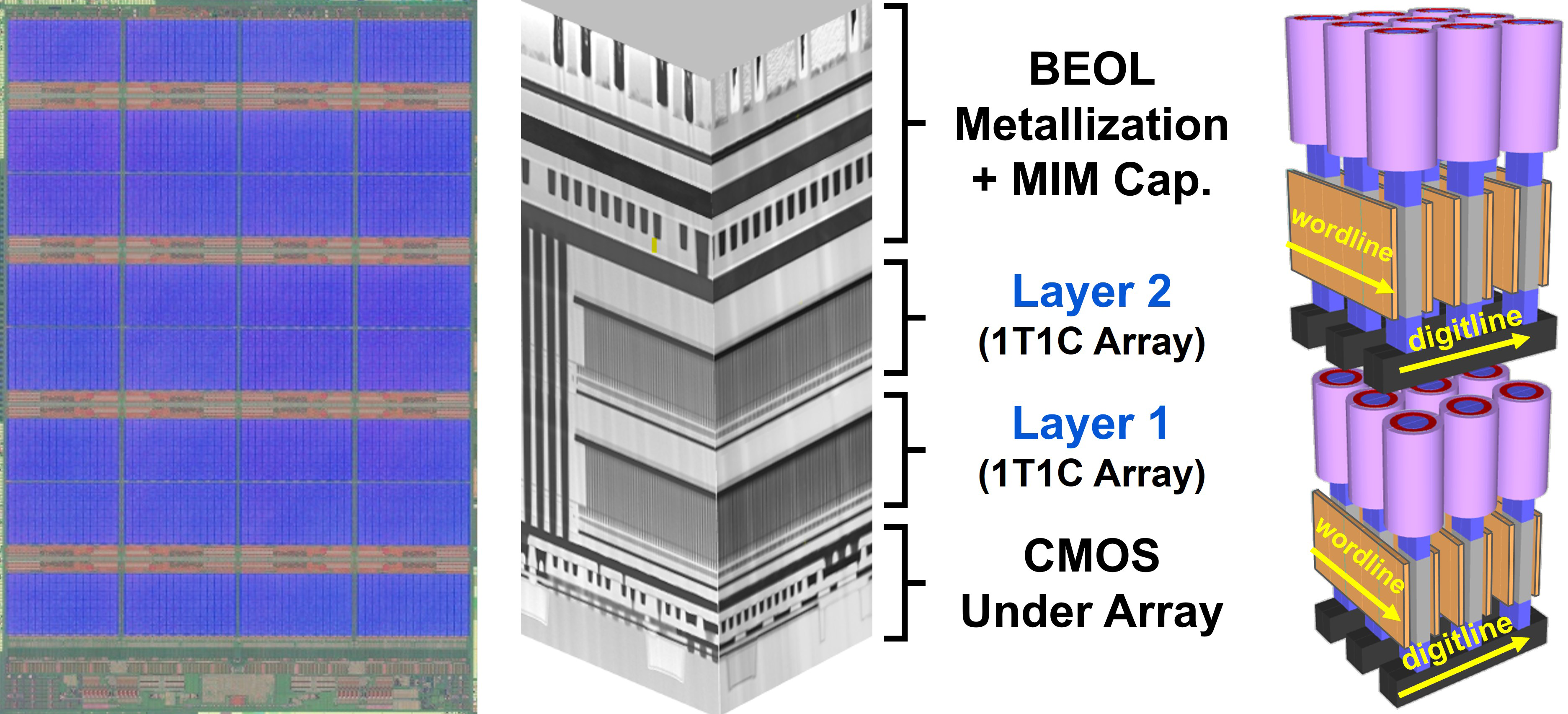
Figure 7. Final die layout (left) and SEM cross-section (center) of a 32Gb NVDRAM with 1T1C memory layers, fabricated on a CMOS array; a schematic diagram of NVDRAM memory arrays (right) shows polysilicon access device with orthogonal word line (WL) and digit line (DL), and ferroelectric memory cells (Paper #15.7, “NVDRAM: A 32Gb Dual Layer 3D Stacked Non-Volatile Ferroelectric Memory with Near-DRAM Performance for Demanding AI Workloads,” N. Ramaswamy, et al, Micron Technology).
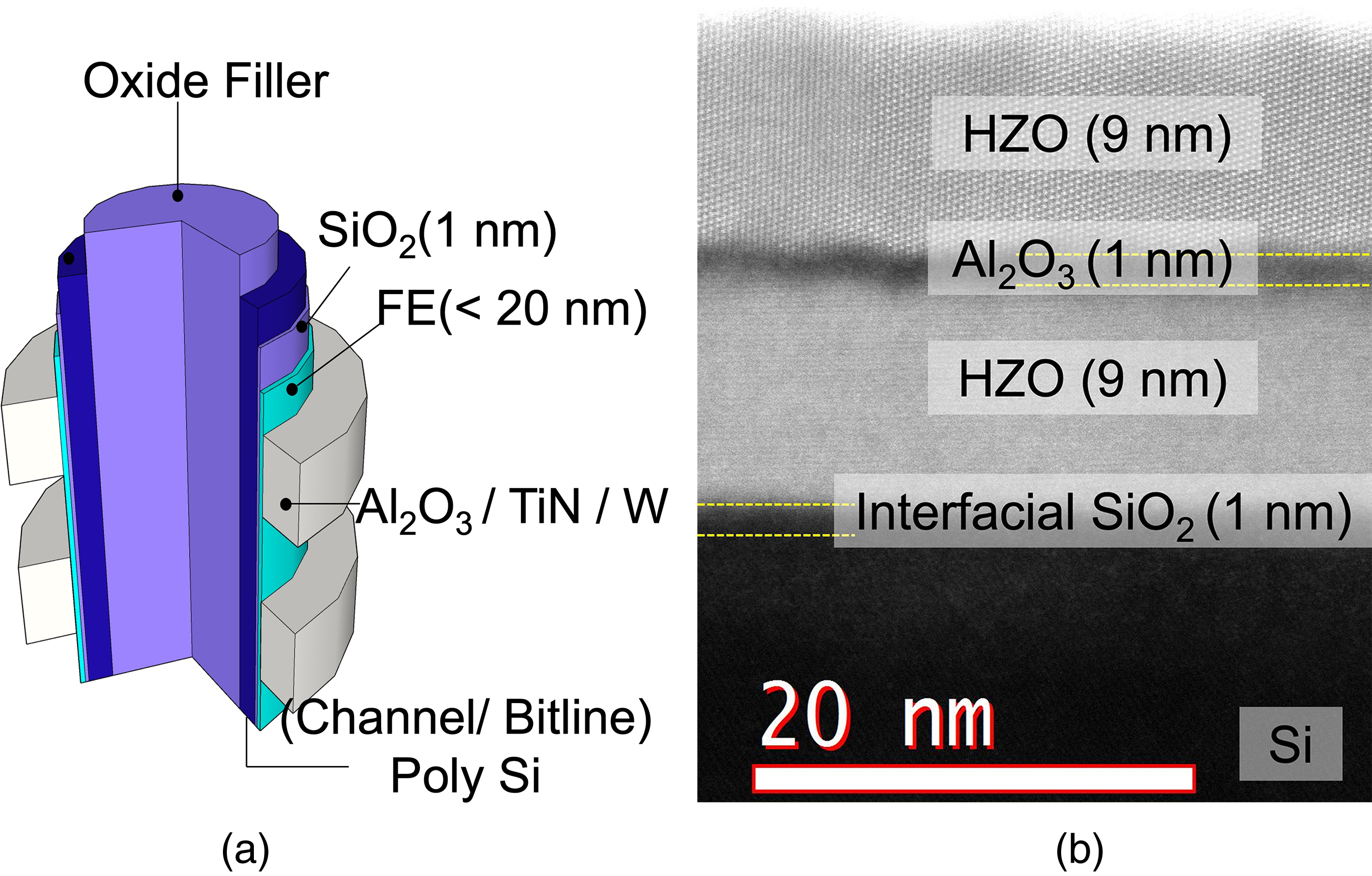
Figure 8. a) An overview of the FE vertical NAND structure. b) A TEM image of the gate stack. A homogeneous 1nm Al2O3 interlayer is clearly visible, suggesting that the formation of the Al2O3 interlayer with uniform thickness and full coverage was achieved (Paper #24.1, “Experimental Demonstration and Modeling of a Ferroelectric Gate Stack with a Tunnel Dielectric Insert for NAND Applications,” D. Das, et al, Georgia Tech/Samsung).
Devices for Neuromorphic Computing
This year for the first time, the IEDM conference has established an entire technical subcommittee devoted to neuromorphic computing, given the strongly growing interest in the field.
GPU-Like Accuracy But With Far Less Energy Use & Inference Time: Large-scale AI models impose ever-increasing demands for computing power and speed in hardware. However, typical 2D compute-in-memory (CIM) architectures suffer from data transfer bottlenecks across the different CIM arrays layers used as processing elements. That’s because each layer’s computation results must use a limited-bandwidth on-chip bus to move between the CIM array and buffers, significantly increasing overall computing time for deep neural networks. In the paper #23.2, “3D Stackable CNTFET/RRAM 1T1R Array with CNT CMOS Peripheral Circuits as BEOL Buffer Macro for Monolithic 3D Integration with Analog RRAM-based Computing-In-Memory,” a Tsinghua University-led team described a monolithic 3D device architecture which integrated buffer arrays right on top of CIM arrays, and dense, fine-grain inter-layer vias (Fig. 9). The 1kb array consists of three functional layers: a 128kb HfO2-based analog RRAM array for the CIM layer; a stackable carbon-nanotube CNT-FET/Ta2O5-based RRAM 1T1R buffer macro layer for data cache; and a Si CMOS logic layer. All devices and circuits were characterized to confirm that each layer worked as designed, and image classification on MLP and ResNET32 networks showed GPU-equivalent accuracy of ∼96.5%, with 39x lower energy consumption and 49.6x less inference time.
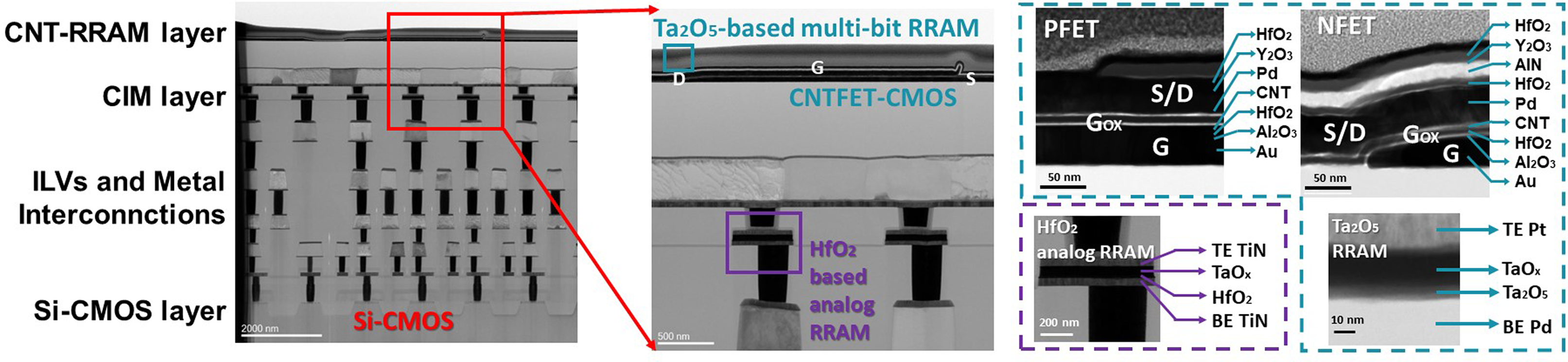
Figure 9. Cross-sectional TEM images of the device (Paper #23.2, “3D Stackable CNTFET/RRAM 1T1R Array with CNT CMOS Peripheral Circuits as BEOL Buffer Macro for Monolithic 3D Integration with Analog RRAM-based Computing-In-Memory,” Y. Zhang, et al, Tsinghua Univ./Peking Univ.)
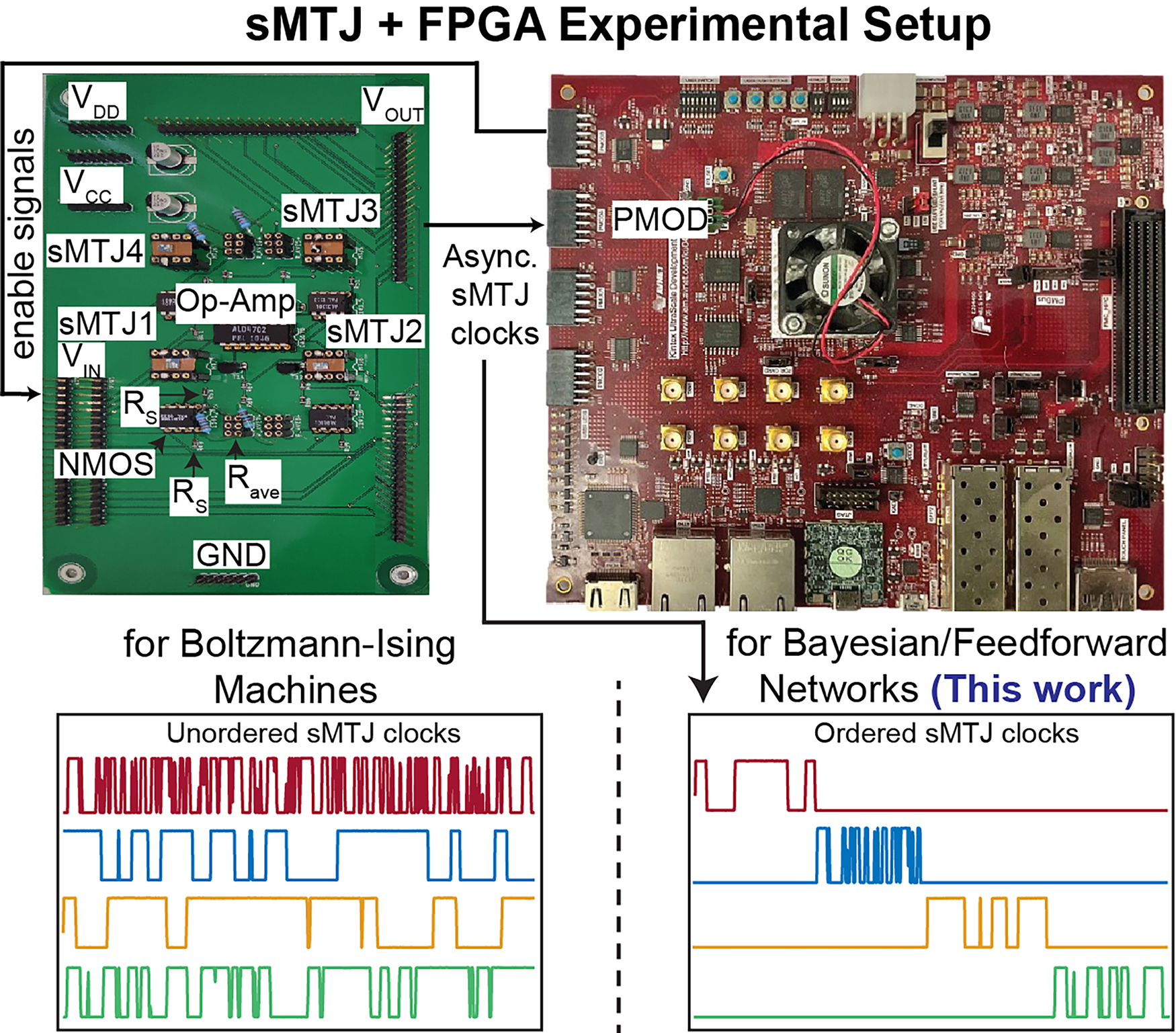
Figure 10. The experimental setup of a printed circuit board (PCB) with 4 sMTJ circuits along with an FPGA. The FPGA sends “enable” signals to the sMTJ circuit inputs (VIN), and asynchronous sMTJ circuit outputs from the PCB are then used to clock pseudo-random number generators (PRNGs). The bottom left of the image shows unordered sMTJ clocks that would be used in traditional Boltzmann machines which are update-order agnostic. The bottom right of the image shows the ordered sMTJ circuit clocks enforced by the enable signals sent from the FPGA. This ordering ensures the ancestral update order for convergence of feed forward networks to the distribution dictated by the Bayes Theorem. (Paper #12.1, “Hardware Demonstration of Feedforward Stochastic Neural Networks with Fast MTJ-based p-bits,” N. Sanjay Singh, et al, UC Santa Barbara/Tohoku Univ.)
Hardware Demonstration of Probabilistic Inference: A feed forward neural network is one where information only moves forward from one layer to the next and does not loop around, with the goal of having an input produce an output that contributes to some sort of prediction. Feed forward neural networks are the backbone of deep learning inference systems, but they impose heavy computational burdens on traditional computing hardware. In the paper #12.1, “Hardware Demonstration of Feedforward Stochastic Neural Networks with Fast MTJ-based p-bits,” a UC-Santa Barbara-led team discussed an inference system for deep feed forward stochastic networks, which led to the fastest probabilistic bits (p-bits) demonstrated to date (three orders of magnitude faster than previous demonstrations). In their system, low-barrier stochastic magnetic tunnel junctions (sMTJ) are used to create probabilistic p-bits, which are then routed to a field programmable gate array (FPGA) circuit to build a hybrid CMOS+sMTJ computer (Fig. 10). The researchers say that scaled versions of the prototype circuit can be used to accelerate a broad range of applications, from deep learning to combinatorial optimization.
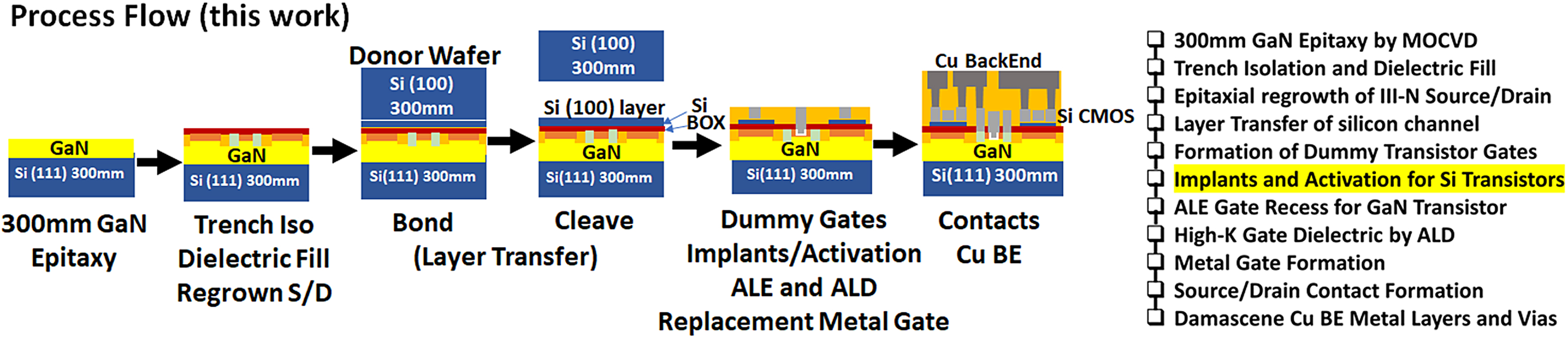
Figure 11. The new process flow for the 3D monolithic integration of GaN and Si CMOS by layer transfer, where the high-temperature activation steps for the Si CMOS transistors are completed before the gate dielectric of the GaN transistors is deposited. (Paper #9.7, “DrGaN: an Integrated CMOS Driver-GaN Power Switch Technology on 300mm GaN-on-Si with E-mode GaN MOSHEMT and 3D Monolithic Si PMOS,” H.W. Then, et al, Intel).
Power Devices
Power Device with CMOS and GaN Channels: Gallium nitride (GaN) devices are attracting great interest for their potential to address the power density/efficiency requirements of data centers and networking platforms. Intel researchers, building on their earlier work to integrate GaN technology with traditional Si CMOS technology, described in the paper #9.7, “DrGaN: an Integrated CMOS Driver-GaN Power Switch Technology on 300 mm GaN-on-Si with E-mode GaN MOSHEMT and 3D Monolithic Si PMOS,” the first integrated CMOS Driver-GaN, or “DrGaN”, power switch, in 300 mm GaN-on-Si technology (Fig. 11). It incorporates an e-mode HEMT and integrated 3D monolithic Si PMOS and potentially enables power delivery solutions to keep pace with the power density/efficiency demands of future CPUs and GPUs. The 180nm DrGaN devices exhibited excellent RDSON (0.8 mΩ-mm2) and leakage (well below 0.1 mA). The researchers will detail a new gate-last process flow for the 3D monolithic integration of GaN and Si CMOS by layer transfer, where high-temperature activation steps for the Si CMOS transistors are completed before the gate dielectric of the GaN MOSHEMT is deposited. This resolves a major hurdle in the 3D monolithic integration of GaN and Si CMOS transistors. This flow also enables the GaN and Si CMOS transistors to share the same backend interconnect stack, eliminating intra-connect resistance and reducing the number of masks. The devices achieved a FOM = 1/(RONQGG) of 0.59 (mΩ-nC)-1 for a 30 nm gate-length GaN MOSHEMT, demonstrating the potential for future scaling of this architecture.
High-Speed Devices
World Record RF Performance & Cryogenic Possibilities: High-speed, power-efficient devices are needed for future terahertz (THz) applications, and for use in cryogenic environments such as quantum computing systems and outer space. But the faster they operate, the harder it is to measure and characterize their performance. At IEDM in 2021, ETH Zurich unveiled an InP/GaAsSb double heterojunction bipolar transistor (DHBT) with a novel emitter fin architecture, which showed record high-frequency performance. At IEDM in 2023, in the paper #34.6, “THz InP/GaAsSb DHBTs with Record 𝑓AVG = 800 GHz: Characterization to 330 GHz,” they described significant advancements in THz transistor characterization and metrology methods up to 330 GHz, which enabled them to determine that their DHBT had an 800 GHz average frequency, a world record for DHBT devices (Fig. 12). They also presented the first cryogenic data for a THz transistor, showing fT/fMAX of 0.57/1.46 THz at 50 K, a world record for any HBT device, opening up new THz applications.
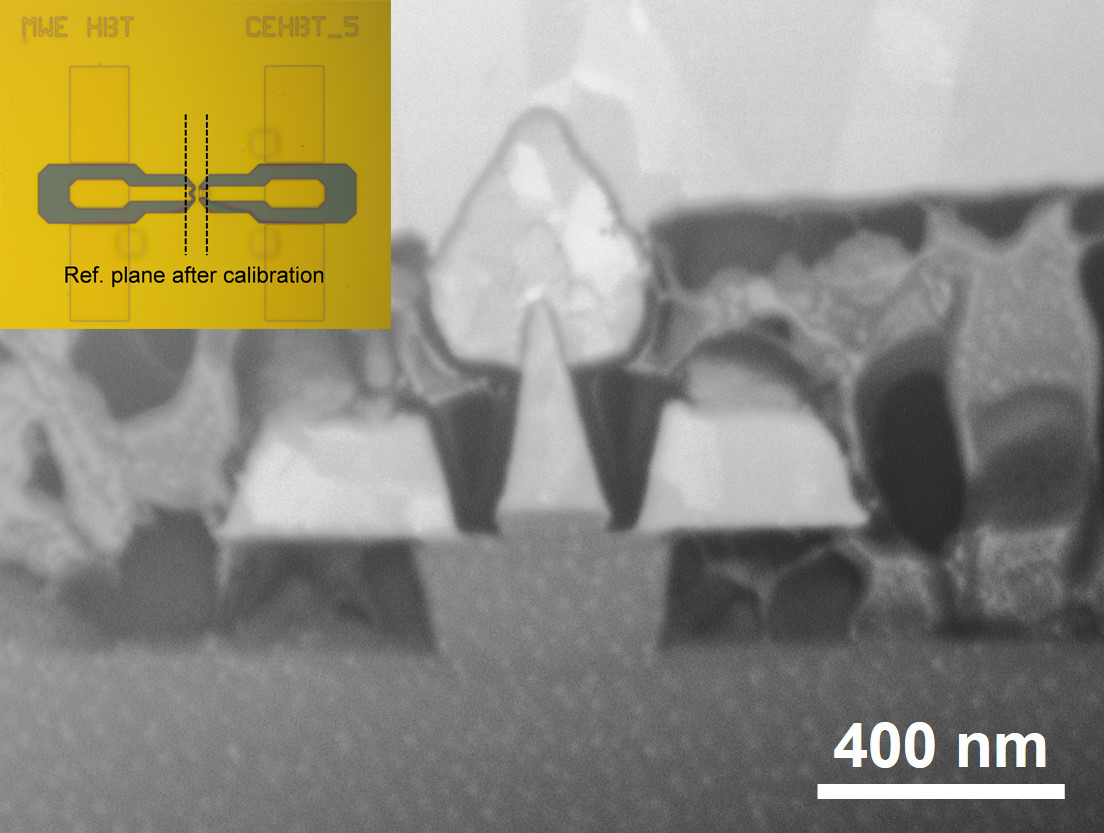
Figure 12. A cross-sectional SEM image of a 175 nm-wide emitter-fin DHBT featuring a 40 nm base access distance. The inset: a top-down microscopic image of a fabricated emitter-fin DHBT with the new shielded co-planar waveguide probe pads for high-frequency measurements. The dashed lines indicate the position of reference planes (Paper #34.6, “THz InP/GaAsSb DHBTs with Record 𝑓AVG=800 GHz: Characterization to 330 GHz,” A.M. Arabhavi, et al, ETH-Zurich/Univ. of Bordeaux).
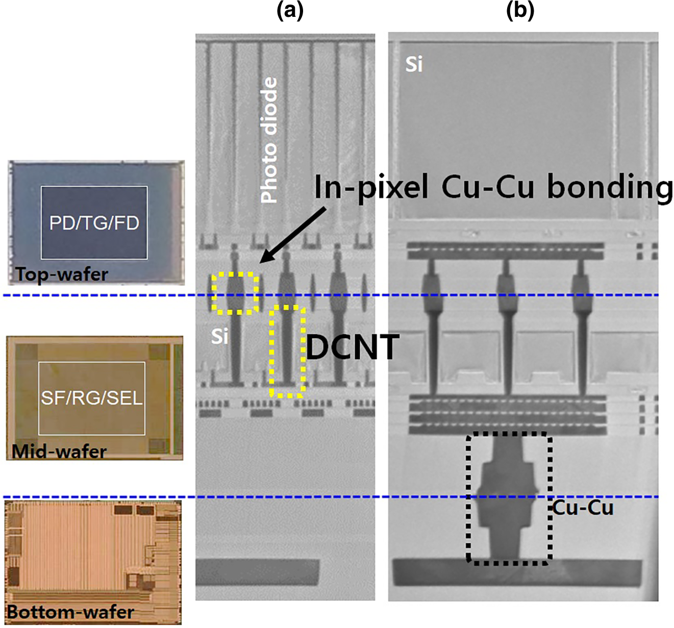
Figure 13. SEM images of the 3-stack structure (longitudinal view): a) the pixel array and (b) the peripheral region (Paper #40.1, “A 0.5 μm Pixel 3-layer Stacked CMOS Image Sensor with Deep Contact and In-Pixel Cu-Cu Bonding Technology,” G-D Ryan Lee, et al, Samsung).
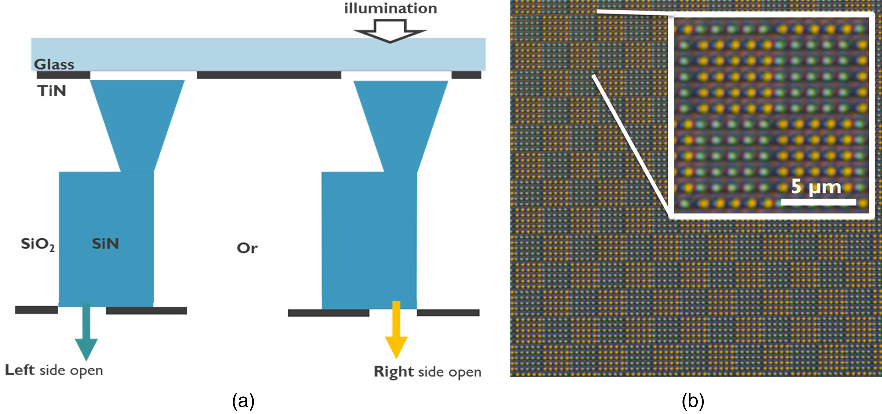
Figure 14. The wafer illuminated with a plane wave of white light; a) visualization of measurement, yellow light exits at the right part of the waveguide, blue light exits on the left; b) RGB camera measurement (100×magn.) of a structure with 620 nm × 250 nm waveguides (pitch = 1 µm) with alternating 5 left-side-open-aperture and 5 right-side-open-aperture waveguides (Paper #8.1, “Wafer-Level-Integrated Vertical-Waveguide sub-Diffraction-Limited Color Splitters,” S. Kang, et al, IMEC/KU Leuven/Ghent Univ.)
Advances in Imaging
Smallest Pixel Ever for CMOS Imagers: A conventional way to get higher resolution from CMOS image sensors (CIS) is to decrease the size of the individual pixels. But smaller pixels are more easily affected by electrical noise, in particular an effect known as random telegraph signals (RTS), and also by parasitic capacitance, which reduces their efficiency in converting light to electrical signals. In the paper #40.1, “A 0.5 μm Pixel 3-layer Stacked CMOS Image Sensor with Deep Contact and In-Pixel Cu-Cu Bonding Technology,” Samsung researchers described a stacked three-layer 64-megapixel CIS architecture with 0.5µm pixels, the smallest ever reported (Fig. 13). A key feature of the device is that it uses copper-to-copper bonding to interconnect pixels from layer-to-layer, which aligns them precisely and thereby reduces the size of the CIS, and also reduces parasitic capacitance. The pixels demonstrated an 85% reduction in RTS noise and a 67% higher gain in light conversion efficiency versus earlier work.
A New Way to Render Colors at Submicron Pixel Sizes: Next-generation CMOS imagers require smaller pixels with higher resolutions. However, smaller pixels capture less light, so increasing their resolution is difficult. A way to capture more light is to split incident light into different wavelengths corresponding to different colors, and then tune those wavelengths to match the color sensitivity of the human eye. In the paper #8.1, “Wafer-Level-Integrated Vertical-Waveguide sub-Diffraction-Limited Color Splitters,” an IMEC-led team described a fundamentally new way to do this at sub-micron pixel sizes (i.e., beyond the fundamental Abbe diffraction limit) using standard backend processing on 300 mm wafers. They built an array of Si3N4 multimode waveguides in a SiO2 matrix. Each waveguide splits a different frequency of light into both symmetric and asymmetric modes, which propagate through the waveguide differently, leading to a unique “beating” pattern between the two modes for a given frequency. This beating pattern is used to represent a certain color (Fig. 14). The researchers said this technique enables further scaling of high-resolution imagers, with the ultimate goal being to detect every incident photon.
A Smart Image Sensor: A Macronix-led team described in the paper #33.2, “3D Monolithically Integrated Device of Si CMOS Logic, IGZO DRAM-like, and 2D MoS2 Phototransistor for Smart Image Sensing” a sequentially stacked device for smart image sensing applications. They built on an 8-inch Si wafer a three-tier monolithically integrated device that included 20nm Si FinFETs, IGZO-based DRAM-like devices, and MoS2 TMD phototransistors with ultra-high responsivity (Fig. 15). With it, they successfully demonstrated a Si FinFET-based logic inverter and NAND and NOR gates; long data retention (>1000s) and low-power working memory for computing-in-memory functions; and a 5x5 array of MoS2 TMD phototransistors with responsivity of >1 A/mW and large tunable photo-gain. This novel platform shows the advantages of BEOL fine-pitch vertical interconnects and can enable small form-factor and ultra-thin smart image sensing systems.
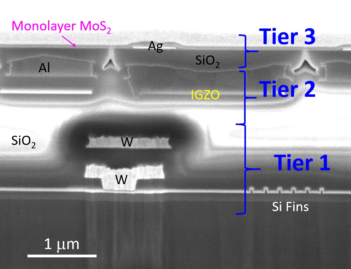
Figure 15. Ccross-sectional SEM view of the 3-tier monolithic 3D image sensor fabricated using a low-thermal budget process; it includes Si FinFETs (Tier 1), 2T0C IGZO devices for DRAM-like operations (Tier 2), and MoS2 phototransistors (Tier 3) (Paper #33.2, “3D Monolithically Integrated Device of Si CMOS Logic, IGZO DRAM-like, and 2D MoS2 Phototransistor for Smart Image Sensing,” F.M. Lee, et al, Macronix/Taiwan Semiconductor Research Institute/National Tsing Hua Univ.)
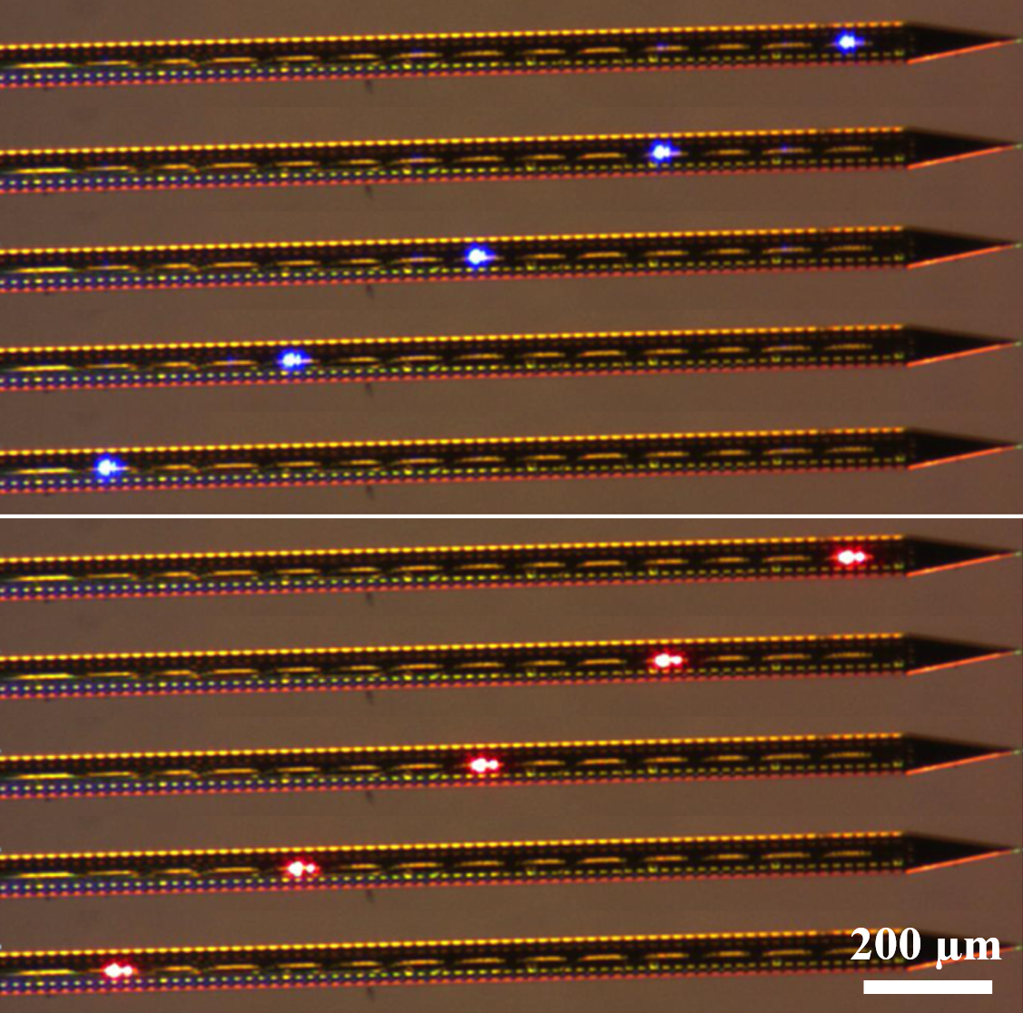
Figure 16. Microscope images of the shank taken during switching between emission sites 1, 4, 7, 10, and 13, at light wavelength 450nm (top), and 638nm (bottom) (Paper #25.6, “Dual-Wavelength Neural Probe for Simultaneous Opto-Stimulation and Recording, Fabricated in a Monolithically Integrated CMOS/Photonics Technology Platform,” P. Neutens, et al, IMEC).
Noteworthy Papers on Diverse Topics
A Flashlight into the Brain: In the paper #25.6, “Dual-Wavelength Neural Probe for Simultaneous Opto-Stimulation and Recording, Fabricated in a Monolithically Integrated CMOS/Photonics Technology Platform,” IMEC researchers detailed a monolithically integrated CMOS/photonics platform, capable of supporting passive and active visible photonics with thermo-optic switches. It incorporates PECVD SiN waveguides built in a 130-nm SOI CMOS process with six layers of aluminum BEOL. They used this platform to demonstrate an implantable CMOS-based neural probe that simultaneously stimulates the brain optically and reads electrical signals from it. It integrates a high-density array of 960 selectable electrodes/384 recording channels with 14 programmable optical emission sites for two visible wavelengths (450 nm and 638 nm) (Fig. 16). Compared to existing multifunctional neural probes having optical transmission and electrical recording capabilities, these probes achieved the largest number of emitters with dual-wavelength operation (a 14x improvement), an order of magnitude higher number of electrodes per shank (>10x improvement), and for the first time, a monolithically integrated readout IC. This technology gives the neuroscience community a powerful tool to use in studies of cell/circuit-specific activity and neural modulation monitoring through optogenetics-based optical tagging. It also can open up opportunities in other applications such as biosensors and super-resolution microscopy.
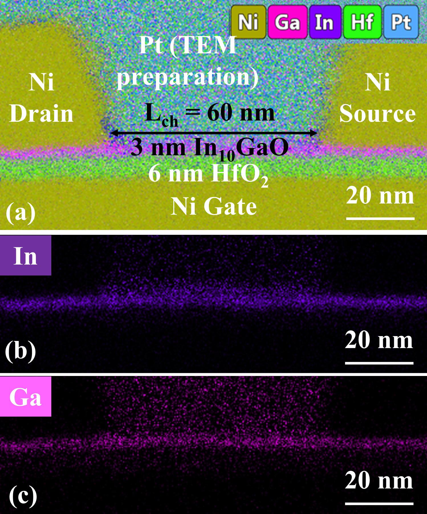
Figure 17. A STEM image of 60nm-channel length InGaO TFTs (a), EDX mapping of indium (b) and gallium (c) (Paper #41.1, “Fluorine Anion-Doped Ultra-Thin InGaO Transistors Overcoming Mobility-Stability Trade-Off,” J. Zhang, et al, Purdue Univ./Xiamen Univ.)
Boosting the Reliability of BEOL-Based Thin-Film Transistors: Building and incorporating ultra-thin CMOS transistors into a chip wiring, or interconnect, as it is fabricated during back-end-of-line (BEOL) processing is a compelling way to build the monolithic, highly integrated 3D devices needed for future neuromorphic, AI, and other computing applications. But while thin-film transistors (TFTs) made from In2O3 are compatible with the low-temperature techniques used in BEOL processing, they suffer from defects such as oxygen vacancies which lead to poor performance and/or temperature/bias instability, impacting their reliability. In paper #41.1, “Fluorine Anion-Doped Ultra-Thin InGaO Transistors Overcoming Mobility-Stability Trade-Off,” a Purdue-led team discussed the use of an alternate channel material (InGaO), doped with fluorine to neutralize defects. They built BEOL-compatible InGaO TFTs with ultra-thin (∼3 nm) 60 nm-long channels (Fig. 17), demonstrating enhancement-mode operation and the highest on/off current performance ever seen in such devices (ION/IOFF ∼1011). They featured a high ION of 418 µA/µm, along with what the researchers call “a remarkably high degree” of temperature/bias stability. The work shows the critical importance of dopants to achieve higher reliability in oxide-based TFTs, and in particular the benefit of using anions (negatively charged) like fluorine in these devices vs. more typically used cation (positively charged) dopants.
Co-Design of Materials & Devices for 2D-Based Logic Circuits: A Spin-FET is a transistor that controls current flow using electron spin states instead of using a charged layer. Although various 2D materials with a wide range of spin-orbit coupling and exotic structural/electrical properties are attractive for designing spin-based transistors and interconnects, the lack of a thorough understanding of spin dynamics has prevented the practical realization of 2D spin logic. In the paper #3.4, “A Materials-Device Co-Design Framework for Realizing Ultra Energy-Efficient All-2D-Spin-Logic Circuits with 2D-Materials,” a UC-Santa Barbara-led team detailed a novel materials–device co-design framework that models many different relevant spin relaxation/dephasing mechanisms, in order to provide realistic design guidelines to both materials and device engineers to advance the state-of-the-art. In particular, the authors revealed that the 2D material graphene has spin diffusion lengths >25 µm, and they showed that circuits based on optimized 2D Spin-FETs outperform their MOSFET counterparts by an order of magnitude in energy delay, and by two orders of magnitude in energy efficiency (Fig. 18).
Other Events in the Time-Frame of 2023 IEDM
In addition to the technical program, several other events took place during 2023 IEDM. On Tuesday, 12 December, there was a career-focused luncheon featuring industry and scientific leaders talking about their personal experiences in the context of career growth. The discussion was moderated by Jennifer Zhao, President/CEO, asm OSRAM USA Inc. The speakers were Ilesanmi Adesida, University Provost and Acting President, Nazarbayev University, Kazakhstan, and Isabelle Ferain, Vice-President of Technology Development, GlobalFoundries. On the same day, the Evening Panel Session was held. It is an interactive forum where experts give their views on important industry topics, and audience participation is encouraged to foster an open exchange of ideas. The panel was moderated by Dan Hutcheson, Vice Chair at Tech Insights. John Chen, NVIDIA was the panel co-organizer. The topic was AI: Semiconductor Catalyst? Or Disrupter? Artificial Intelligence (AI) has long been a hot topic. In 2023 it became super-heated when large language models became readily available to the public. The 2023 IEDM brought together industry experts to have a conversation about how AI is changing the semiconductor industry and to ask them how they are using AI to transform their efforts. The panelists were Pierre Paulin, Synopsys; Ira Leventhal, Advantest; Chris Lin, TSMC; Nicole Saulnier, IBM; and Anantha Sethuraman, Applied Materials. The topics were wide-ranging, from how AI will drive demand for semiconductors, to how it’s changing design and manufacturing, and even to how it will change the jobs and careers of those working in it.
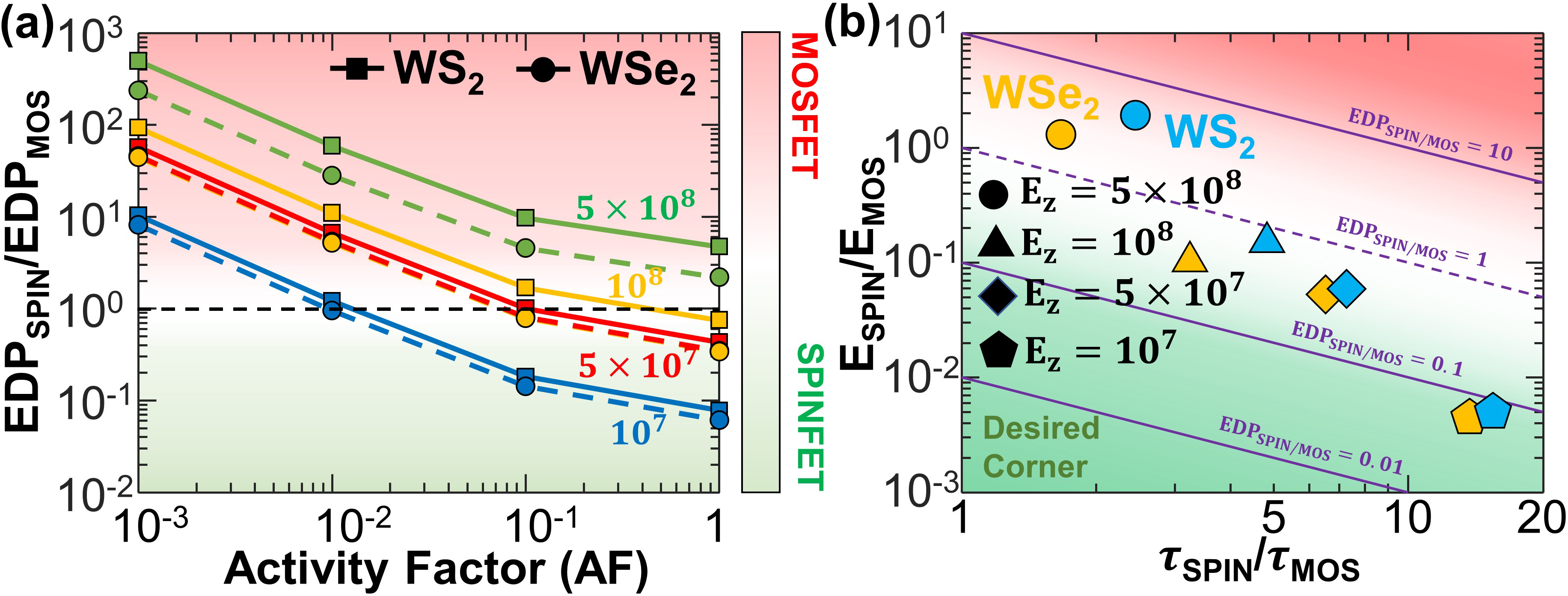
Figure 18. Energy-delay-product (EDP) ratio of Spin-FET-to-MOSFET with p-type WS2 and WSe2 channels, as a function of circuit activity factor (AF) for out-of-plane electric fields (EZ) of 107, 5×10⁷, 108, and 5×10⁸ V/m at 100K. The black dashed line (ratio = 1) demarcates the regions where Spin-FETs (green) and MOSFETs (red) show more EDP benefit (Paper #3.4, “A Materials-Device Co-Design Framework for Realizing Ultra Energy-Efficient All-2D-Spin-Logic Circuits with 2D-Materials,” S. Zhang, et al, UC-Santa Barbara/Zhejiang Univ.)
Three other events are also worth mentioning, namely:
We hope that this overview will be useful to you and that it will encourage you to seek information on topics of interest to you in the 2023 IEDM materials, which will be available through IEEE Xplore. We are looking forward to meeting you at IEDM 2024!
For registration and other information, visit www.ieee-iedm.org. Follow also IEDM via social media:
Your comments are most welcome. Please write directly to the Editor-in-Chief of the Newsletter at
daniel.tomaszewski@imif.lukasiewicz.gov.pl
A Review of the 2023 IEEE International Integrated Reliability Workshop (IIRW):
the Flagship Workshop on recent advances in Integrated Electronics Reliability

The aim of IIRW is to provide an annual international forum for the presentation and discussion of recent advances in all aspects related to electronics reliability. As the demand for higher computational efficiency increases and diversifies, the level of reliability required for modern devices, circuits, and systems is rapidly increasing, fostered by economic drivers such as the automotive industry, the advent of artificial intelligence, edge computing, high-performance computing, and aerospace. Therefore, more than ever before, a deeper interaction among reliability engineers, technologists and device experts, circuit designers, and system developers is necessary. In this scenario, IIRW provides the ideal setting in which the attendees can meet at the beautiful Fallen Leaf Lake, CA, USA, to exchange ideas over four days in a friendly and informal environment. The event was held in person, October 8–12 2023. Notwithstanding the echoes of the global pandemic, the widespread economic instabilities, the semiconductor business stagnation, and the critical war scenarios in Eastern Europe, the event was joined by participants from all over the world, achieving the second-highest attendance in the last ten years (excluding 2020 and 2021 in which IIRW went fully virtual), confirming the attractiveness of the workshop for the semiconductor reliability community. The IIRW conference was financially sponsored by the IEEE Electron Devices Society and Reliability Society. In addition, world-class companies in the field of micro- and nano-electronics co-sponsored the conference:
Given the unique and secluded location of the conference, many attendees had to face a long journey to the Stanford Sierra Conference Center in Fallen Leaf Lake. Thus, the first day of the conference was dedicated to welcoming the attendees. A dinner provided ground for the attendees to start getting to know each other, before the traditional Sunday Night Tutorial, a “techlite” lecture delivered after dinner—this year the topic was the role of analog electronics in music.
The conference was then officially opened by the General Chair of the conference, Prof. Francesco Maria Puglisi (University of Modena and Reggio Emilia, IT), and by the Technical Program Chair, Dr. Charles LaRow (Intel Corporation, US) who welcomed the attendees and delivered the commemorative plaques to the awardee of the 2022 IEEE IIRW Best Student Paper Award (Tommaso Rizzi, IHP Microelectronics GmbH, DE) and to the General Chair of the 2022 IEEE IIRW, Dr. Matthew Hogan (Siemens Digital Industry Software, US). After the introduction and conference opening, the Keynote presentation by Dr. Elisa Vianello (CEA-Leti, FR) followed. Dr. Vianello’s talk was entitled “Harnessing the potential of imperfect resistive memory technologies for efficient computing” and gave the attendees a vision of how it is possible to actually leverage on the intrinsic reliability issues of emerging devices such as resistive memories to realize dependable and reliable neuromorphic and in-memory computing systems, which are pivotal for the much awaited pervasive introduction of ubiquitous artificial intelligence on energy-constrained devices. Dr. Vianello showed how resistive random access memory (RRAM) holds tremendous promise for the development of innovative neuromorphic and in-memory computing platforms by enabling highly parallel, low-power, and low-latency computations, offering significant advantages in terms of energy efficiency and computing power for AI workloads compared to traditional systems. She then showed how implementing such computations using RRAM devices presents challenges due to practical device limitations, including variability, quantization error, and limited endurance, to then focus on various strategies for effectively integrating unreliable devices into neuromorphic and in-memory computing paradigms, capitalizing on the unique imperfections of RRAM devices leading to new neuromorphic circuits and Bayesian nanoelectronics.
Figure 1. A picture from the keynote presentation by Dr. Elisa Vianello (CEA-LETI) entitled “Harnessing the potential of imperfect resistive memory technologies for efficient computing”.

Figure 2. A group picture of the panelists who contributed to the Reliability Experts Forum, together with, on the right, the REF moderator (Dr. Zakariae Chbili, Intel Corporation) and the two REF Co-Chairs (Michael Waltl, TU Wien—Suresh Uppal, Rivos Inc.).
On top of that, 20 contributed papers with deep insights and high-level technical content were presented during the conference in 7 sessions focused on specific reliability topics (Transistors, Power and RF, Device and Circuit, BEOL, Metrology and Characterization, and Memory). The sessions also included 8 invited talks by prestigious speakers on different topics, ranging from 2D materials reliability to new challenges in packaging. Additional 13 contributed papers were presented in the Poster Session, hosted after dinner on the third day of the conference, in which lively discussions between the poster presenters and the attendees took place, providing the ideal ground for ideas exchange and networking. All contributed papers can be found in the proceedings published on IEEEXplore.
A peculiar feature of IIRW is that tutorials are not offered in parallel sessions on a dedicated day, but are rather disseminated during the whole conference, each placed in a strategic time slot according to the subject in order to give the audience, especially students, the necessary tools to fully engage in ensuing highly technical discussions on a given topic. In 2023, tutorials were given by Cristian Zambelli (University of Ferrara, IT—“Emerging Memory Reliability”), Stephen Moxim (NIST, US—“Connecting the Dots between Analytical Magnetic Resonance Results and Semiconductor Device Reliability”), and Gennadi Bersuker (M2D Solutions, US—“From Chaos to Order: Evaluating Memristor Technologies for neural network implementations”).
IIRW has evolved over the last years to include a unique event called the “Reliability Experts Forum” (REF), where a pool of world-class reliability experts from both industry and academia contributes to two themed panels on hot topics in reliability, involving the audience in a wide and lively discussion. Attendees registered for the conference had the chance to attend all of the scheduled activities, including the REF, the tutorials, the discussion groups, all the invited and contributed oral presentations, and the poster session. In 2023, IIRW hosted the sixth edition of the REF on the third day of the conference, to which eleven experts gathered in a day-long discussion articulated in two panels to debate about i) Aging in Advanced Nodes and Hot Carrier Degradation; and ii) VMAX and technology scaling. The event was moderated by Dr. Zakariae Chbili (Intel Corporation, US). The first panel was honored by the presence of Dr. Miaomiao Wang (IBM, US), Dr. Erik Bury (imec, BE), Prof. Souvik Mahapatra (IIT Bombay, IN), Dr. Minjung Jin (Samsung, KR), and Dr. Andreas Kerber (Intel, US) as panelists, sharing their expertise with the audience. After a short presentation by each of the panelists, the audience engaged in an energetic discussion that involved the other panelists as well. Different aspects related to the main topic were discussed, including a general introduction to the topic, advanced modeling strategies, consequences at the device and circuit level, and industry-level strategies to deal with the unpredictability of the aging response in the most advanced nodes. The second panel, held in the afternoon, has seen panel contributions from Dr. Jeffrey Hicks (Intel Corporation, US), Dr. John Faricelli (AMD, US), Dr. Bonnie Weir (Broadcom, US), Dr. Jen-Hao Lee (TSMC, TW), and Dr. Patrick Justison (GlobalFoundries, US). Notwithstanding the long and vivid discussions held in the morning, stimulating questions and discussions came from the audience as a result of the short presentations from the panelists. Perspectives on the factors truly limiting the supply voltage reduction in scaled technologies and on strategies to circumvent them were given by both fab leaders and design experts, offering a diversified but clear and comprehensive picture.

Figure 3. Introducing the “Aging in Advanced Nodes and Hot Carrier Degradation” panel of the Reliability Experts Forum.
In addition, the conference hosted four discussion groups. After the dinner on the second day of the conference, two parallel discussion groups took place. The first was entitled “Talent Pipeline from Academia to Industry”, was moderated by Dr. Zakariae Chbili (Intel Corporation, US) and focused on the current worldwide crisis of education in semiconductors and the so-called talent shortage, at the center of structural initiatives such as the US and EU Chips Acts. The second was instead focused on “Challenges in Electromigration with New Materials and Constructs” and was led by Prof. Lado Filipovic (TU Wien, AT). The presence of renowned experts in the field of electromigration made the discussion group a success. Two additional parallel discussion groups took place after the dinner on the fourth day of the conference. The first was entitled “Aging in Advanced Nodes” and was moderated by Dr. Theresia Knobloch (TU Wien, AT). Echoing the lessons learned during the first REF panel, the discussion pinpointed the expectation of the reliability community on the next generation of devices for ultimate scaling in terms of aging mechanisms, reliability margins, and possible new phenomena to carefully consider to guarantee a smooth transition toward both the beyond CMOS and the angstrom era. The second was entitled “TDDB: Is the Power-law the end of the road?”, and was moderated by Dr. Bonnie Weir (Broadcom, US). Both the academic and the industrial perspectives were discussed, proposing ideas and methodologies to appropriately assess the TDDB margin. New insights derived from recent studies on AC breakdown and on the microscopic modeling of oxide integrity together with remarks from the second REF panel were brought into the discussion, bringing the community one step closer to potentially answering the long-standing question that gave the title to the discussion group.

Figure 4. The Technical Program Chair (left, Dr. Charles LaRow, Intel Corporation) and the General Chair (right, Prof. Francesco Maria Puglisi, Università di Modena e Reggio Emilia).
The conference also included a social program. At the end of each day, characterized by an intense technical program, the attendees were welcomed in the “Old Lodge”, a cozy cabin in which a friendly reception took place, promoting networking among the attendees. In addition, the whole afternoon of the fourth day of the conference was free of technical activities for the attendees to enjoy the unique location in which the event took place. Many returning attendees escorted first-time IIRW participants in hiking on amazing routes around the lake and up to Mount Tallac to enjoy a breathtaking view. The conference was then officially closed before lunch on the last day, with the announcement of the IIRW 2024 conference, which will take place in Fallen Leaf Lake, October 6 through 10, 2024. The deadline for a two-page abstract submission is June 16, 2024, and the preliminary Call for Papers is available at www.iirw.org.
In summary, IIRW 2023 was an inspiring event with ample participation and a rich and stimulating program. The IIRW community is looking forward to another exciting edition in Fallen Leaf Lake, CA, USA, October 6 -10, 2024.
Francesco Maria Puglisi
2023 IEEE IIRW General Chair
The 5th IEEE International Flexible Electronics Technology Conference 2023
The 5th IEEE International Flexible Electronics Technology Conference (IFETC) 2023, hereafter referred to as the “conference,” was held during 14–16 August 2023 at the DOUBLETREE BY HILTON hotel, San Jose, California, USA. This in-person conference featured outstanding presentations of contributed and invited papers and contributed posters by researchers from industry and academia as well as students from 17 countries worldwide along with five Plenary talks by prominent multi-disciplinary experts from the industry and academia over three scheduled days of the conference.
The conference was inaugurated on Sunday, 13 August with pre-conference tutorials in the morning and short courses in the afternoon aimed at students, practitioners, and individuals transitioning to the broad technical area of flexible/printable electronics. The tutorials and short courses were presented by internationally recognized researchers and technologists from industry and academia. The topics and instructors have been carefully chosen to have broad appeal to IFETC 2023 participants including students as well as experts in the field.
The topics of the three tutorials included:
The topics for three short courses were:
The main conference opened on Monday, 14 August morning with the Plenary Session presenting three featured talks:
On Day 2, Tuesday, 15 August, the conference sessions began with a Plenary talk,
The conference technical program was organized into a total of 17 sessions with multiple parallel sessions featuring papers on a broad range of flexible/printable electronics device/manufacturing-related topics including sensors, displays, and in general large area flexible electronics systems within eight technical areas:
Each session included contributed and invited papers on cutting-edge flexible/printable electronics device/manufacturing-related topics within the scope of the above-selected eight technical areas. In this brief review, no attempt is made to summarize these papers that are available on IEEEXplore: https://ieeexplore.ieee.org/xpl/conhome/10254736/proceeding. The following basic trends are observed from the presented papers at the IFETC 2023.
A large number of presentations were on Materials, Devices, and Processing showing a huge R&D effort leading to the manufacturing of transistors and sensors on flexible substrates. The papers include metal-halide perovskites flexible transistors, microscale photodetectors, and sensors; In-Ga-Zn-O source-gated thin-film transistors on a flexible polyimide film substrate; sol-gel-based p-type copper-oxide high-performance thin-film transistor by doping the precursor solution with an alkali metal for flexible electronics; and one-dimensional and bidimensional materials technology to achieve devices and circuits on flexible substrates for large scale integration.
The papers on Energy Harvesting and Storage included presentations on high-efficiency ultrathin transition metal dichalcogenides (TMDs) flexible (WSe2) solar cells using novel approaches in semiconductor device design, TMD materials growth, and photonic engineering; high-efficiency III-V flexible photovoltaic (PV) devices grown by multi-chamber hydride vapor phase epitaxy (HVPE); triboelectric nanogenerators (TENGs) for harvesting ambient mechanical energy to produce electrical power and operate self-powered sensors and wearable electronics using advanced 3D printing techniques; and materials and techniques to fabricate flexible supercapacitors and batteries.
There were, also, a large number of presentations on Sensors, Actuators, and Bioelectronics. The presentations included skin-interfaced wearable biosensors; wearable sensors for non-invasive sport monitoring; multilevel fabric mold textures film-based flexible pressure sensors; high-density, superior-performance and large-scale TFT-based optical/pressure/biosensors; thin-film temperature sensor on flexible polyether ether ketone (PEEK) fabric substrate with possible applications in automotive, fuel, and gas filtering monitoring; polymer-based sensors for gastrointestinal temperature and gas monitoring; battery-free wearable electrochemical sweat sensors using energy harvesting modules such as TENGs, biofuel cells (BFCs), and solar cells; biomimetic polymer electronics for intimate bio-interfaces; flexible hybrid electronics wearable sensors for mental health monitoring; inkjet-printed flexible sensors, for diabetic foot ulcer monitoring; flexible Tactile Sensors; and so on.
In continuation, there were a good number of excellent presentations on the practical implementation of flexible/printable electronics in manufacturing and productization with concentrated efforts on circuits and systems integration; functionalities, performance, and reliability engineering as well as emerging applications, specifically in the healthcare industry.
Along with the IFETC 2023, the 14th International Conference on Computer-Aided Design for Thin-Film Transistor Technologies (CAD-TFT) was co-located in San Jose on 16 August 2023. And, there were excellent presentations in CAD-TFT 2023 from industry and academia including numerical process and device simulation of TFT as well as compact TFT modeling for circuit analysis.
In addition to excellent contributed and invited paper sessions on the above briefed diverse topical areas of flexible/printable electronics, on Monday, 14 August morning, EDS president, Ravi Todi formally introduced the 75th Anniversary of the Transistor, a commemorative book published by Wiley-IEEE Press in July, 2023. And, the evening featured the Women in Electron Devices Society and Young Professionals session to delve the power and influence of women and young professionals into. The session “Diversity in the Next 75 Years of the Transistor: Off to a Good Start;” on Tuesday, 15 August featured a luncheon talk, “Marketing the Unknown,” by Sri Peruvemba of Marketer International, Inc., San Ramon, California, USA, and an evening interactive panel session, “Why and How Investment Would Accelerate Growth in Flexible/Printable Electronics Industry?,” offering a forum for deep-dive discussions on the potential growth of flexible/printable electronics industry around the globe.
Samar Saha
Prospicient Devices, USA
IFETC 2023 General Chair
IRDS–Factory Integration Roadmap
1. Introduction
The Factory Integration (FI) chapter of the IRDS is dedicated to ensuring that the manufacturing infrastructure of the microelectronics represented by Si-based semiconductor devices contains the necessary components to produce items at affordable cost and high volume in a sustainable manner. Realizing the potential of Moore’s Law and novel device structures beyond traditional CMOS-based devices requires taking full advantage of device feature size reductions, new materials, yield improvement to near 100%, wafer size increases, and other manufacturing productivity improvements. This in turn requires a factory system that can fully integrate additional factory components and utilize these components collectively to deliver items that meet specifications determined by other IRDS international focus teams (IFTs) as well as cost, volume, and yield targets. Preserving the decades-long trend of a 30% per year reduction in cost per function [1] also requires capturing all possible cost reduction opportunities. These include opportunities in front-end as well as back-end production, facilities, yield management and improvement, increased system integration such as up and down the supply chain, improving environmental health and safety performances, and supporting sustainable microelectronics production. FI challenges play a key role in microelectronics realizing its full potential for society and many FI technology challenges are becoming limiters to achieving major technology milestones for microelectronics.
In particular, the FI chapter addresses several challenges/issues that threaten to slow the industry’s growth, including:
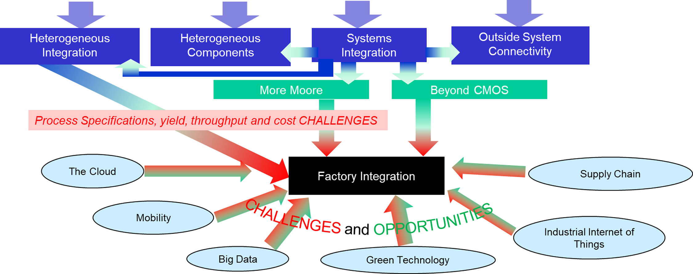
Figure 1. Societal Forces Impacting Challenges and Opportunities in FI [6].
2. FI Drivers and Technology Targets
Societal driving forces and trends such as mobile devices and the Internet of Things (IoT) are impacting all areas of the IRDS, however, as shown in Fig. 1, these factors impact the evolution of FI from two perspectives, namely:
An analysis of the first perspective can be found by studying the roadmaps developed by other IRDS focus groups as illustrated in Fig. 1. The same analysis can be applied to determine how the FI roadmap addresses the related tighter process requirements. With respect to the second perspective, the following is an example of how some of these drivers directly impact FI:
3. Vision of Future Technology
The future of microelectronics manufacturing FI is imbued in large part in the tenets of “Smart manufacturing” (SM) and Industry 4.0 (I4.0). Key tenets of this migration include leveraging Big Data infrastructures, integrating with the supply chain network, leveraging advanced analytics, improving the use of cyber-physical systems (CPS), improving the use of real-time simulation through realizing the “digital twin,” and relying on a knowledge network for using subject matter expertise (SME) in an increasingly collaborative environment [7]. These terms are expounded upon in the Smart Manufacturing sub-chapter of the FI roadmap. This migration is associated with a number of challenges ranging from moving from reactive to a predictive/prognostic mode of operation to addressing security associated with data sharing.
4. Evolution and Extension of Factory Integration Scope
Microelectronics manufacturing extends across several manufacturing domains. FI’s scope is microelectronic manufacturing including fabrication in front-end and back-end. The FI Focus Team has addressed the evolution of FI by providing an extensible roadmap that 1) focuses on the commonality of certain functional areas, 2) supports roadmaps for specific functional and physical areas, 3) addresses societal drives identified above, and 4) provides for improved synergy with Environmental, Safety, Health, and Sustainability (ESH/S) as well as Yield Enhancement (YE) objectives, requirements, and solutions. The evolution of the Factory Integration roadmap scope is depicted in Fig. 2.
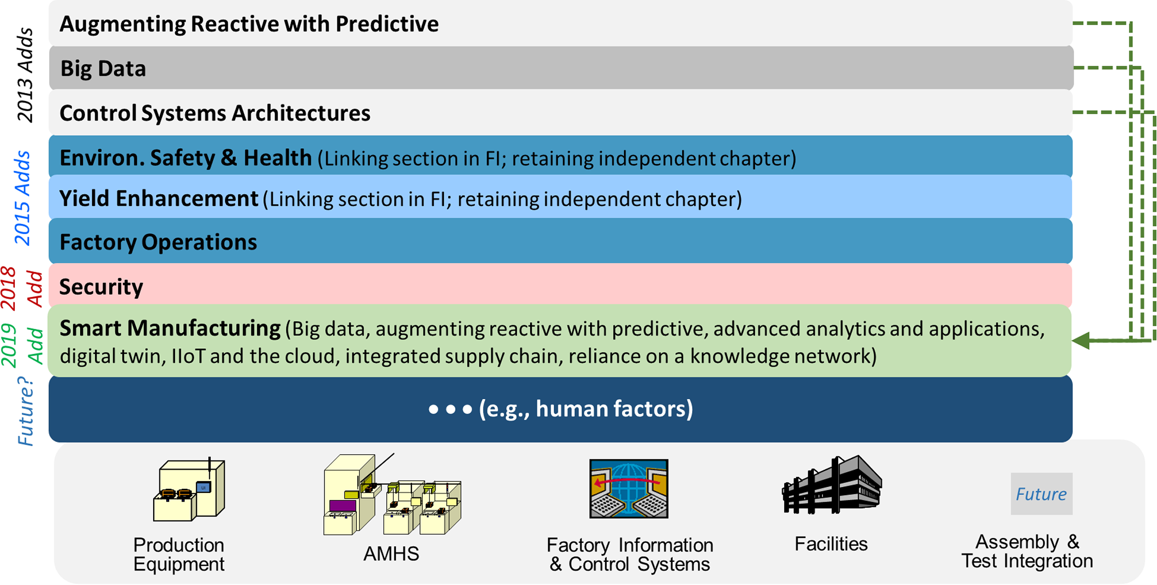
Figure 2. Factory Integration scope extension and evolution.
The following are key factors contributing to and demanding the extension and evolution of FI scope.
The technologies addressed by the FI roadmap need to provide solutions that can be used to leverage economy of scale and resource pooling. Scaling of production volumes tends to ease the typical FI issues that have an impact on cost such as 1) “design to volume production” lead time improvement, 2) yield improvement, 3) productivity waste reduction, 4) higher process controllability, and 5) reduction in utilities, power consumption and emission with even more progressive targets. Wafer size increase had also been one of the major contributing factors for the cost scaling of the semiconductor device, but this process stalled in 2015 when increasing challenges related to device functional scaling made it too difficult to continue scaling across two fronts. While it is possible that Si wafer size increase from 300mm to 450mm returns to become a high-priority FI topic again in the future, it is not deemed as a priority at least in the near or medium term, or even as far as functional performance scaling of devices continues.
FI scope traditionally includes some consideration on design and materials used for production equipment and the facility systems to ensure the level of ESH performance as required by regulations or Fab owners’ operation policies. Implementation of Sleep mode functions for production equipment augmented with upgrades of the host-equipment message communication to support host-controlled sleep mode is an example of this type of ESH/S and FI crosscut technology requirement.
There are increasing demands from ESH/S to FI to provide better data integration and sharing not only within Fab components but also across the supply chain. For example, in order to meet near future environmental targets such as science-based targets (SBTs) in line with the goals of the Paris Agreement, collecting all the required data from every piece of production equipment and the overall facility systems operations will become paramount. This will almost certainly result in a need for more sensors and sensing methods, which can be translated into FI requirements in its production equipment as well as facility sections. Along with more sensors, networking, and data integration among sensors, equipment, and every level of control system up to the entire Fab or even a site level are to be required for better optimization of utilization efficiency of utilities (e.g., electricity or cooling water) and production materials (e.g., process chemicals/gasses) evaluated against normalized environmental impact indexes (e.g., GHG emission from Fab operation or net amount of equivalent CO2 emission). These impact indexes are called Scope 1, 2, and 3 and address the entire supply and value chain. Another ESH/S challenge example is the need to verify that semiconductor device manufacturing is compliant with ESH-related regulatory requirements, such as GHG reporting rule by the US EPA, which also is driving dedicated sensors and sensor methodologies as well as data and control integration solutions.
The yield of semiconductor manufacturing has been a critical factor in determining the viability of each chip production technology, which is also the key objective of the Factory Integration (FI) chapter of the IRDS, namely producing semiconductor devices at affordable cost. Yield enhancement has been traditionally enabled by continuous improvement of the manufacturing equipment and process on one hand and by improvement of the cleanliness of the process environment and materials used on the other. There is a common understanding that systematic defect control is being addressed by IC Device Manufacturers (IDMs) working directly with the technology providers, which leaves unaddressed challenges in the space of random defect (contamination control), which is covered by the Yield Enhancement (YE) chapter of the IRDS, and the ability to respond to Yield excursion which is addressed in the Factory Integration (FI) chapter. Additionally, the need to understand and control systematic defects by the IDMs poses data availability and quality requirements to FI.
Ongoing evolution of consumer products such as voice-activated home assistant devices and autonomous driving vehicles is heavily relying on various types of sensors, the IoT, and artificial intelligence enabled by wide varieties of semiconductor and other microelectronics devices (e.g., MEMS) This evolution has introduced the semiconductor-industry outlook of exponential growth possibility with more volatility. Today’s semiconductor firms need to be more flexible, with a greater focus on research and development; increased functionality; and shorter, more efficient production times. Such changes have led to significant challenges to the traditional semiconductor supply chain, which has been accustomed to predictable demand for qualities and quantities. In order to meet the challenge posed by the evolution, all levels of production, including semiconductor device manufacturers themselves, foundries, assembly and testing firms, material providers, component, and processing equipment supplier companies will need to form an interactive, organic supply chain to meet new demands for greater capacity, performance, quality, and manufacturing costs. FI roadmap should support the application of technologies in the supply chain integration space and its challenges.
In addition to the issues stated above, the need for data transfer protocol across the supply chain for traceability of quality issues to solve productivity losses (i.e., yield losses and production equipment overall operational efficiency reduction) while maintaining data security also poses significant challenges to FI.
Furthermore, as an important part of the supply chain for the users of microelectronics devices, (e.g., automotives or medical equipment) field yield or latent yield, which is often identified by the occurrence of a failure of the microelectronic devices in the field, can be considered as a supply chain issue within FI scope.
5. Smart Manufacturing in the Microelectronics Industry
As noted earlier, Smart Manufacturing (SM) or Industry 4.0 concepts such as cyber-physical systems, virtual copies of real equipment and processes, and decentralized decision-making are expected to create a smarter factory [2,3]. While the literature base for SM and I4.0 is wide and varied, common themes or tenets of SM are present that help provide an understanding of the whole SM and I4.0 space, as well as the structure for the organization of SM roadmap elements [7]. An SM vision for the microelectronics industry is shown in Fig. 3 [4,5]. Note that, while the tenets of SM and I4.0 are not industry-specific, each industry has its unique challenges and opportunities. IRDS FI Chapter envisions microelectronics industry-specific variations of the SM.
The microelectronics manufacturing is a unique industry characterized by high process precision requirements and a highly dynamic production environment, process and equipment complexity, high degrees of intellectual property (IP) encapsulated in production equipment, manufacturing processes, and analytical solutions, and a business model that focuses on development and maintenance of fab-wide solutions [4]. These characteristics result in unique requirements (or at least reprioritization of requirements) and challenges in realizing smart microelectronics manufacturing.
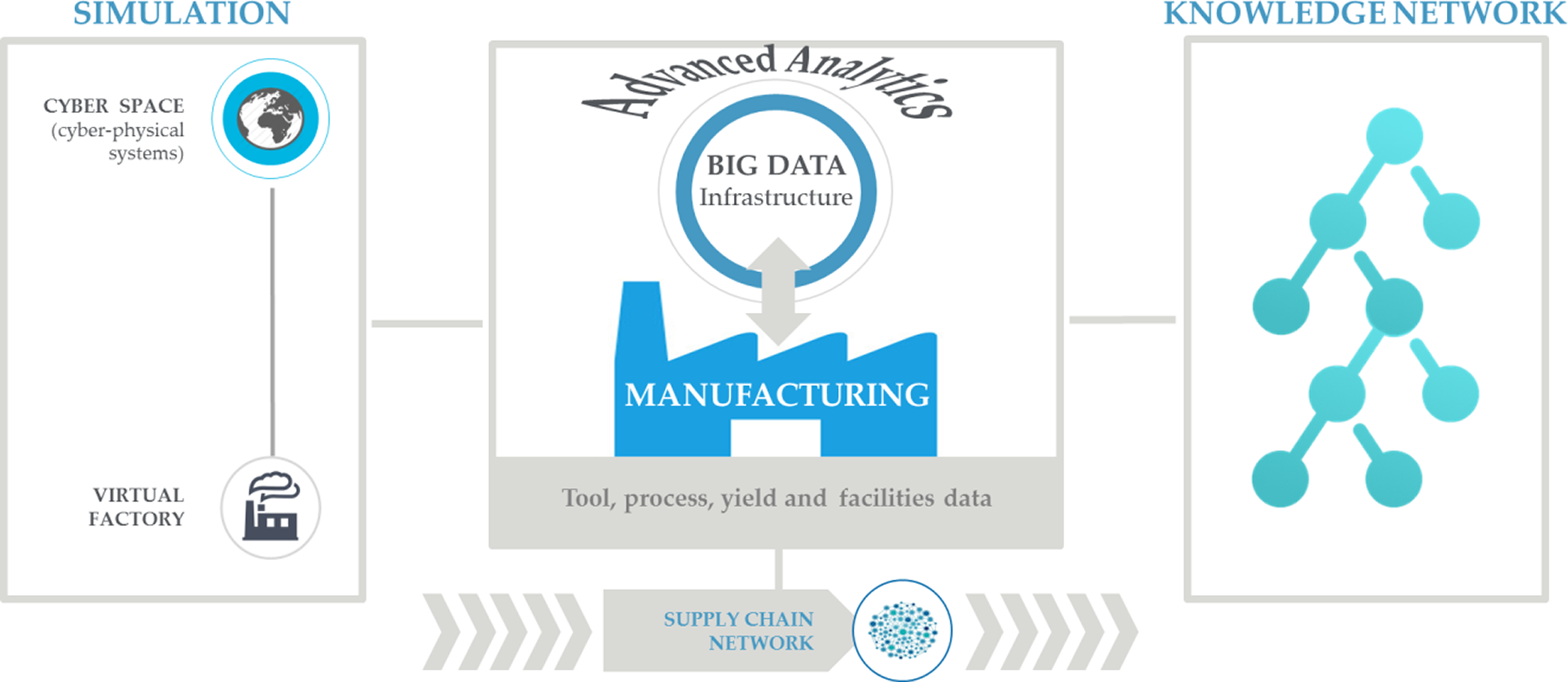
Figure 3. A Smart Manufacturing vision for the microelectronics industry [4].
Based on an understanding of the general focus areas of SM combined with the unique needs of the microelectronics manufacturing ecosystem, the IRDS FI chapter is maintaining a roadmap for each of the following SM tenets:
As a first step to address this issue, SM literature efforts have tried to define the analytics capabilities in terms of dimensions and apply these dimensions to the needs of particular applications, as shown in Fig. 4 [4]. It is expected that this definition will help guide the analytics roadmap in future FI chapters.
| Technology | Definition | NOTE | |
| Advanced Process Control (APC) | The manufacturing discipline for applying control strategies and/or employing analysis and computation mechanisms to recommend optimized machine settings and detect faults and determine their cause [8] |
|
|
| Basic APC Technologies | Fault Classification | The technique of determining the cause of a fault once it has been detected [8] | |
| Fault Detection (FD) | The technique of monitoring and analyzing variations in tool and/or process data to detect anomalies. FD includes both univariate (UVA) and multivariate (MVA) statistical analysis techniques. [8] | ||
| Fault Detection and Classification (FDC) | Combination of FD and FC [8] | ||
| Fault Prediction (FP) | The technique of monitoring and analyzing variations in process data to predict anomalies [8]. | ||
| Run-to-Run (R2R) control | The technique of modifying recipe parameters or the selection of control parameters between runs to improve processing performance. A ‘run’ can be a batch, lot, or an individual wafer. [8] | ||
| Statistical process control (SPC) | The technique of using statistical methods to analyze process or product metrics to take appropriate actions to achieve and maintain a state of statistical control and continuously improve the process capability [8] | ||
| Technologies Extended upon APC | Equipment Health Monitoring (EHM) | The technology of monitoring processing tool (equipment) parameters to assess tool health as a function of deviation from its normal (baseline) behavior. EHM itself is not basically predictive in nature but is often a component of predictive and/or controlling systems [5] | |
| Predictive Maintenance (PdM) | The technology of utilizing process and equipment state information to predict when a tool or a particular component in a tool might need maintenance, and then utilizing this prediction as information to improve maintenance procedures. This could mean predicting and avoiding unplanned downtimes and/or relaxing planned downtime schedules by replacing predetermined schedules with predictions. PdM solutions as defined herein address the entire maintenance cycle, from predicting maintenance through addressing recovery from maintenance events towards returning to production [5]. | PdM for equipment or a particular equipment component can be managed at the equipment level or fab level as fab-level coordination of individual tool maintenance can contribute to fab-level productivity improvement. | |
| Predictive scheduling | The technology of utilizing current and projected future information on tool and factory state, capabilities, wafer/work in process (WIP), schedule, dispatch, and orders to predict and improve scheduling of a system (tool, group of tools, floor, fabs, etc.). | ||
| Virtual Metrology (VM) | The technology of monitoring information across the fab (e.g., tool and metrology) to predict process or end-of-line yield [8] | While E133 uses ‘VM’ as the acronym of Virtual Metrology, FI roadmap refers it by (VMet) | |
| Yield Prediction (YP) | The technology of monitoring information across the fab (e.g., tool and metrology) to predict process or end of line yield. | ||
Table 1. Definitions of APC and APC-extended capabilities.
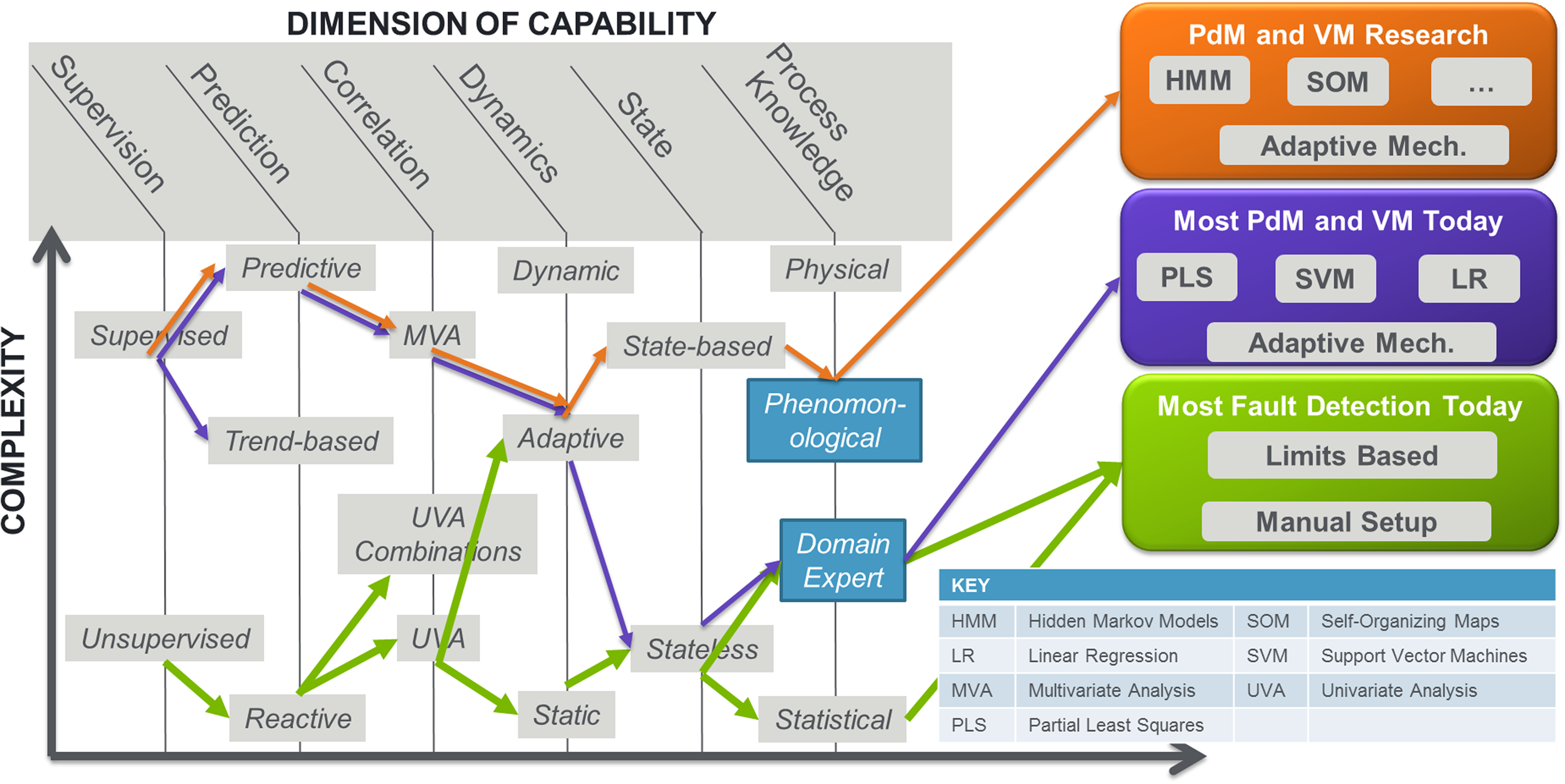
Figure 4. Example of Defining the Dimensions of Analytics Capabilities [4].
6. Future of Analytics: AI and Further Exploitation of Big Data
Emergence or re-emergence of AI and other new Big Data-friendly analytics are expected to play an important role in realizing many of the FI objectives. Before diving into the recent and continuing evolution in this topical area, let’s define a few keywords in this topical area;
Artificial neural networks (ANN), an example of an AI type of analytics, have been around for decades and such AI analytics have seen a resurgence as part of the Big Data evolution. DL, which is a technique very similar to structured ANN, leverages hierarchical abstraction for improved quality and speed when applied to high-volume data analysis required, for example, to optimize production equipment conditions for the process performance level necessary to achieve desirable yield. The main drawback of DL-based techniques is their relative inability to incorporate SME in model development and maintenance as well as their requirements for large amounts of data to develop models.[13,14] The models developed by the DL technique are often not explicitly available and difficult to assess, while the context richness and dynamics involved in semiconductor manufacturing analysis hinder DL-based techniques from fully leveraging large and consistent data volumes provided by the advancement of Big Data capabilities in the industry. Some research efforts have focused on combining SME with AI techniques, an approach that holds promise for future application on the manufacturing floor [12–14].
Another Big Data-friendly analytical technique is background analysis by solutions often termed “crawlers.” In a similar manner to “Web crawlers”, these applications mine data in the background, looking for patterns of interest in sensor trace data, such as a part nearing the threshold of its normal operation range to abnormal. They inform a relevant control system such as a PdM manager or equipment engineering system (EES) so that appropriate action can be taken to reduce unpredicted downtime.
As the microelectronics manufacturing industry migrates towards the full realization of SM, it is clear that the role of analytics empowered by Big Data advancements, in achieving yield goals while maximizing throughput and lowering cost, becomes larger.
7. The Need of Addressing the Data Sharing Conundrum
If the microelectronics industry is to fully realize the benefits of SM and especially AI analytics within the industry, it must recognize that there is a need to address a broad commercial problem. The benefits offered by SM depend upon accurate and reliable ML-based models that require large volumes of data for training and timely availability of appropriate data for inferencing. For example, DL-based models often need the use of larger and/or raw data sets to enable capabilities such as feature profiling. Within the microelectronics manufacturing Fab and across its supply chain, the data needed by AI analytics is owned by many stakeholders and may contain details that reveal proprietary IP or commercial liability. As a result, there is an inherent bias against data sharing at a level that can support the necessary modeling. In one example of many occurrences of anti-data-sharing tendencies, optimizing the complex, end-to-end process requires AI to manage the volume and rate of data flowing, but that in turn requires data from every process step to train effective models. If that data is coming from sensors integral to the operation of a process step, it may leak equipment vendor IP, so sharing with the equipment user (i.e., device manufacturer or foundry) could be seen as problematic. Meanwhile, data about the overarching process is proprietary to the user, so can’t easily be shared with the equipment vendors.
The IRDS FI focus team believes, however, that this is an opportunity for exactly the type of pre-competitive collaboration that the industry has excelled at previously.
In this respect, unlocking data for AI applications will necessitate technology requirements being established in the FI roadmap for a trusted mechanism for consuming data that is owned by multiple stakeholders, which can both ensure that stakeholder rights are protected and realize appropriate data analysis that can be of value.
8. Conclusion
The Factory Integration focus area in the IRDS is in a rather unique position in the entire set of IRDS roadmap reports in that it does not address directly any device features (e.g., structure and material) or performance requirements for devices or systems composed of devices as the core enabler of realizing each system’s functions and performances. Further, it does not address technologies that directly enable device features that are required for a device technology to fulfill its functional targets such as processing speed, latency, or retention of value. Instead, the FI roadmap addresses necessary components across the manufacturing ecosystem such as facility system performance and equipment control architecture criteria allowing newer modes of operation such as energy-saving operation of production equipment. As part of this charter, the FI roadmap is increasingly addressing the incorporation of Smart Manufacturing (SM) tenets for microelectronic device production and its supply chain. While the potential of “smarter” semiconductor manufacturing realized through the adoption and optimization of the common SM tenets in microelectronics manufacturing and its supply chain has at least partially been realized, there are certain obstacles, namely security and data sharing concerns, that have prevented this industry from becoming the leading adopter and beneficially of the technologies offered by SM.
It is and continues to be the IRDS FI focus team’s core mission to evaluate those SM-related challenges and come up with technology requirements needed for addressing the challenges as well as potential pathways to satisfy the technology requirements.
9. Acknowledgments
The authors acknowledge the valuable contributions of the IEEE IRDS Factory Integration focus team members to the IEEE IRDS Factory Integration Roadmap. Furthermore, we acknowledge the contributions of Erik Collart, Terry Cox, Leo Kenny, and Slava Liebman for their insights and lively discussion on full expanse of the FI topical area including the crosscut with ESH/S and YE.
References
[1] “The 2015 Intel decomposition of manufacturing cost per transistor, using equation (2), is shown as Figure 3, and in Table 1.” Has Moore’s Law Been Repealed? Empirical Analysis of Innovation in Semiconductors Kenneth Flamm/ University of Texas at Austin, Industry Monetary Fund WWW.IMF.Org
[2] Project of the Future: Industry 4.0, Germany Ministry of Education and Research, Available on-line: http://www.bmbf.de/en/19955.php.
[3] Kagermann, H.; Wahlster, W. INDUSTRIE 4.0 Smart Manufacturing for the Future. Germany Trade and Invest, 2016.
[4] J. Moyne and J. Iskandar, “Big Data Analytics for Smart Manufacturing: Case Studies in Semiconductor Manufacturing,” Processes Journal, Vol. 5, No. 3, July 2017. Available on-line: http://www.mdpi.com/2227-9717/5/3/39/htm
[5] “Factory Integration,” in International Roadmap for Devices and Systems: 2020, IEEE 2020. [Online]. Available: https://irds.ieee.org.
[6] International Roadmap for Devices and Systems, 2016 Edition: Factory Integration White Paper. Available online: https://irds.ieee.org/images/files/pdf/2016_FI.pdf.
[7] J. Moyne, “Bringing subject matter expertise and analytics together in solutions for microelectronics smart manufacturing: Consensus, domains, and approaches,” APC Conference XXXI, San Antonio, TX. Oct. 2019. [Online]. Available via http://apcconference.com.
[8] J. Moyne, H. Hajj, K. Beatty and R. Lewandowski, “SEMI E133: The process control system standard: Deriving a software interoperability standard for advanced process control in semiconductor manufacturing,” IEEE Trans. on Semiconductor Manufacturing, vol. 20, no. 4, pp. 408-420, Nov. 2007
[9] J. Moyne et al., “A Requirements Driven Digital Twin Framework: Specification and Opportunities,” in IEEE Access, vol. 8, pp. 107781-107801, 2020, doi: 10.1109/ACCESS.2020.3000437.
[10] J. Moyne, S. Mashiro, D. Gross, “Determining a security roadmap for the microelectronics industry,” Proceedings of the 28th Annual Advanced Semiconductor Manufacturing Conference (ASMC 2018), Saratoga Springs, New York, May 2018, pp. 291-294
[11] What is Artificial Intelligence (AI). https://www.ibm.com/topics/artificial-intelligence
[12] I. Kovalenko et al., “Toward an Automated Learning Control Architecture for Cyber-Physical Manufacturing Systems,” in IEEE Access, vol. 10, pp. 38755-38773, 2022, doi: 10.1109/ACCESS.2022.3165551.
[13] Lammers, D. “Big Data and Neural Networks: New Drivers for the Semiconductor Industry,” Nanochip Fab Solutions, Vol. 12, No.1, 2017, pp. 22-28
[14] Vogel-Walcutt, J.J; Gebrim, J.B.; C. Bowers; Carper, T.M.; Nicholson, D. “Cognitive Load Theory vs. Constructivist Approaches: Which Best Leads to Efficient, Deep Learning?” Journal of Computer Assisted Learning, 2010. Available online at https://onlinelibrary.wiley.com/doi/10.1111/j.1365-2729.2010.00381.x
1 Deep Learning is a technique that is very similar to structured artificial neural networks and leverages hierarchical abstraction for improved quality and speed of high-volume data analysis [13].
Hybrid 2D/CMOS microchips becoming a reality
It’s accurate to say that silicon electronics are ubiquitous nowadays. From toasters to fans, electric brushes, fridges, and of course cameras, TV sets, phones, and computers have some microchip within them to deliver power, control engines or carry out computations that were unachievable, and almost unthinkable, merely a few decades ago. The importance of these microchips is being manifested in the current efforts by many countries in the semiconductor ecosystem to retain or gain some sovereignty in this geopolitical element of ever-increasing importance; the digitalization of society is one characteristic element of the XXI century.
Even though there are better-suited materials for electronics, with better carrier mobility or direct bandgaps, silicon still dominates thanks to its maturity, versatility, and cheapness. The transistor is the cornerstone on which all this progress rests. Moore’s law, Dennard scaling, and ultimately Scale Length Theory, propelled the silicon technology forward as the backbone of modern electronics, pushing it to its very limits. All these developments expanded its application ranges from its early analog origins as an amplifier, with bipolar transistors, to modern logic powering data centers and AI applications with CMOS technology, which is probably the apex of silicon technology. Physically, from a manufacturing point of view, this has been achieved through miniaturization, with many different and very inventive solutions: channel strain engineering, high-K dielectrics, and channel body thinning, to name a few. There were many important advancements introduced in planar architectures, before jumping into alternative architectures such as fins, nanosheets, and nanoribbons. We are however reaching the fundamental physical limits of this approach, manifested in the so-called short channel effects, where it is clear that a paradigm change is needed if we want to keep boosting performance at the transistor level.
Now, 2D materials are entering the scene. The advent of graphene and other atomically thin materials was a lucky strike when electronics needed it the most. This new class of materials presents ultrathin bodies, with excellent electrostatic control, without showing any mobility degradation when aggressive channel scaling is introduced; furthermore, ultrapure graphene devices show mobilities exceeding that of Si and III-V materials by many orders of magnitude. Graphene was precisely the first one to be isolated, sparking interest in the field. Later, a myriad of different materials were established through extensive research, such as hexagonal boron nitride (h-BN) and transition metal dichalcogenides (TMDs). Moreover, these new materials have complementary properties such as insulating, semiconducting, and metallic behaviors, which allow them to mimic conventional electronic design. However, the two-dimensional nature of these materials enables exploiting many different exotic effects, such as multiexciton states, valley polarizations, and superconductivity (among others) which could give rise to potential new devices in the future, expanding the range of capabilities of electronics.
The first studies on 2D-layered materials for electronics produced the material by mechanical exfoliation of bulk crystals using scotch tape. The flakes produced by this method have uncontrollable lengths of a few to hundreds of micrometers, and variable thicknesses of a few nanometers [1]. However, the ease and cheapness of this method allowed 2D materials research to be somehow democratized. Then, the 2D-layered flakes were stuck onto a small substrate made of SiO2/Si or Al2O3/Si, and electrodes were patterned using electron beam lithography to form the devices. Using this method, transistors, capacitors, barristers, and memristors (among others) were created, and breaking performance were reported. That includes, for example, transistors with 2D semiconducting channels that exhibit current on/off ratios order of 108, high charge carrier mobility of 700 cm2/Vs, and low subthreshold swing of 74 mV/decade [2]. However, mechanical exfoliation cannot be used to produce 2D layered materials at the wafer level, and hence all those studies lack relevancy for the industry. Nevertheless, they produced valuable knowledge that allows an understanding of the potential and limitations of the 2D materials.
In the following years, different methods to produce synthetic 2D layered materials were developed. Among them, liquid phase exfoliation (LPE) and chemical vapor deposition (CVD) attracted a lot of attention due to their high throughput, as they were able to coat 300 mm wafers. The first method (LPE) produces a solution containing a high density of 2D layered flakes, which can be deposited on any wafer easily using different methods like spin coating (among others) [3]. This results in thin films with thicknesses from tens to hundreds of nanometers formed by a mesh of 2D layered flakes. Although the junctions between the different 2D-layered flakes contain defective bonds and impurities that degrade performance, the LPE method can be used to fabricate large devices on arbitrary substrates, and it is ideally suited for the production of large-area circuits and sensors for all kinds of objects in the Internet of Things. Some studies reported the construction of transistors and logic gates [4], but their size was too large (hundreds of micrometers). No study has ever reported the fabrication of multiple nanosized electronic devices via LPE, and it is expected that the large inhomogeneities within the 2D materials film would lead to a low yield, large variability, and poor reliability (because the atoms in such film are easy to move when an electrical field is applied).
More interestingly, the scientific community and more importantly, the industry have been able to synthesize continuous 2D layered materials at wafer-scale using chemical vapor deposition (CVD). Using this approach, the thickness of the 2D material can be controlled much more accurately, and the density of native defects (such as lattice distortions, missing bonds, strained bonds, impurities, thickness fluctuations, surface roughness, wrinkles, and cracks) is also much lower [5]. The main drawback of this method is that it requires high temperatures above 800 ºC, which impedes direct growth on pre-processed silicon microchips. For this reason, some efforts are focused on synthesizing 2D semiconducting materials on empty or blank wafers and employing them as a channel in transistors, building the entire chip on them—in a standard silicon microchip technology, deposition of the semiconducting Si is also the first step. IBM used this approach in 2011 to fabricate a sheet of monolayer graphene on a SiC wafer (at 1400 ºC) and then built a radiofrequency mixer containing one graphene transistor and two inductors [6]. However, the capabilities of such types of small circuits are very limited, and the topography of the SiC makes it difficult to obtain low device performance variations.
There is however a second approach, in which the graphene films are grown in a substrate material and then transferred onto a different, target wafer. This transfer approach is much more versatile due to the decoupling of the growth substrate and the target wafer, which enables the integration of these materials at the back-end-of-line (BEOL) and its monolithic integration with silicon circuitry. In 2014, IBM (again) proposed the integration of 2D materials in silicon samples containing pre-patterned circuitry [7]. Using this approach, the 2D material is used only for the required operation, and the rest of the operations can be carried out according to the well-optimized traditional silicon technology. The circuit presented contained four inductors, two resistors, two capacitors, and three transistors (with a monolayer graphene channel). All the elements were patterned but the transistors were left with source and drain contacts exposed at the last metallization layer and without channel. Then, the graphene was synthesized by CVD method on a Cu substrate at 1000 ºC and transferred on the pre-patterned silicon wafer using a room temperature process. Finally, the graphene film was patterned, filling only the required channel area between the source and drain. The resulting circuit exhibited a high cutoff frequency of ∼16 GHz, but far from ideal estimations for standalone graphene transistors (∼100 nm at 240 nm gate length), which indicates that further optimization of processing parameters was needed, and the size of the transistors was large (channel size of 10.8 μm2), which still requires miniaturization efforts.
The very relevant work by Goosens et al. [8] at Instituto Ciencias Fotónicas de Cataluña (ICFO) used a similar approach when monolayer graphene was transferred on silicon samples containing CMOS read-out circuits and constructed an array of 388 × 288 image sensors sensitive to light wavelengths between 300 and 2,000 nm. The graphene played the role of the conductive path and covered an area of ∼105 μm2 in each pixel. The authors estimated that the yield was 99.8% by measuring if the resistance was low (correct) or high (failure). The reason for such success was that in such large areas, the presence of local defects in the graphene does not produce an open circuit, which opens up the way for certain applications in which the structures don’t need to be aggressively scaled down.
The 2D Experimental Pilot line [9], a project consortium from the European Commission that involves several top European institutions, is trying to automatize the production of wafers containing 2D materials. They offer multi-project wafer tape-outs which the customers can fabricate at least once per year at prices affordable to academics and start-ups. While the consortium is strongly working on the integration of other 2D materials such as TMDs, with semiconducting properties that enable logic applications, the project currently offers only circuits containing monolayer graphene, which limits the types of circuits that can be fabricated, and almost impedes the use of 2D materials for data management.
In 2023, a breaking study published in Nature presented the fabrication of the first hybrid 2D/CMOS microchips for high-integration-density data storage and computation [10]. The group led by Prof. Mario Lanza at the King Abdullah University of Science and Technology (KAUST) integrated h-BN at the BEOL of a silicon microchip containing CMOS transistors of the 180 nm node. The h-BN had a thickness of ∼18 layers, each of them made of B and N atoms with in-plane covalent bonding and separated from each other by a 0.33 nm van der Waals gap, leading to a total thickness of ∼6 nm. The CMOS circuit was designed using Cadence software and fabricated on a 200 mm wafer in an industrial foundry. However, the wafer was terminated after the 4th metallization step and left without passivation. Hence, the vias coming from the CMOS transistors were exposed to the atmosphere. The wafer arrived at KAUST laboratories with a native oxide, which was removed via wet etching to expose the metallic vias before transferring the ∼18-layer-thick h-BN on top. Finally, top Au/Ti electrodes and interconnections were created using photolithography, electron beam evaporation, and lift-off.
The h-BN stack was therefore sandwiched between two metals, the W via coming from the transistors and the top Au/Ti electrodes, forming arrays of one-transistor-one-memristor (1T1M) cells (see Figure 1). The size of the Au/Ti/h-BN/W memristor was only 0.053 μm2, which was determined by the diameter of the vertical W via (∼260 nm). In terms of performance, the authors demonstrated nonvolatile bipolar resistive switching for millions of cycles, and the yield was above 80%. The size and endurance of these devices were like that of memristors integrated with commercial products, such as nonvolatile memories [11–13], with the added advantage of a higher controllability of the on/off resistance window and the possibility of inducing threshold-type resistive switching (useful for the implementation of selectors and electronic neurons). One of the clues of this study was the use of multilayer 2D material, which is much stronger than monolayer from a mechanical point of view and does not crack so easily during transfer [5]. The 1T1M structure is the basic cell for data storage and computation in memristive circuits, and it can be used as nonvolatile memory, for in-memory computation, or as electronic synapse in crossbar arrays for vector-matrix multiplication (which is a key operation in artificial neural networks).
Figure 1. Fabrication of hybrid 2D/CMOS memristive microchips. a, Photograph of the 2 cm × 2 cm microchips containing the CMOS circuitry. b-c, Optical microscope images of a part of the microchip containing a 5 × 5 crossbar array of 1T1M cells, as received and after fabrication (respectively). The size of the squared pads is 50 µm × 50 µm. d-f, Topographic maps collected with atomic force microscopy of the vias in the 5 × 5 crossbar arrays on the wafers as-received, after native oxide etching, and after the transfer of the h-BN sheet (respectively). g, Optical microscope image of a finished 5 × 5 crossbar array of 1T1M, i.e., after h-BN transfer and top electrodes deposition. h, High-angle annular dark-field cross-sectional scanning transmission electron microscope image of a 1T1M cell in the crossbar array. The inset, which is 20 nm × 16 nm, shows a cross-sectional transmission electron microscopy image of the Au/Ti/h-BN/W memristor on the via; the correct layered structure of h-BN can be seen. Reproduced with permission from reference [10], copyright Springer-Nature 2023.
It is worth noting that transistors with channels made of 2D materials have been fabricated in the past and that, while large devices tend to work relatively well [14], channel lengths below 100 nm result in a prohibitive degradation of performance, variability, and yield [15]. On the contrary, memristors are devices in which the current flows across the device’s weakest location, making it almost insensitive to process imperfections creating point defects [5, 10]. The size of these 2D-materials-based devices (0.053 μm2) [10] is several orders of magnitude smaller than those previously reported on-chip using monolayer graphene (>10 μm2) [6-8], and the technology readiness level is relatively high for this kind of materials.
Another breakthrough in hybrid 2D/CMOS integration is exemplified in the recent paper, also published in 2023, by Soikkeli et al. [17], in which monolayer graphene was also integrated at the BEOL of a CMOS wafer with readout circuitry to create monolithic graphene biosensors, where the active element was a graphene resistor which was driven and read by the silicon circuitry sitting underneath it. This was the first example of monolithic integration of graphene for biosensing applications. In this case, the 200 mm analog CMOS wafers were sourced from a commercial foundry, fabricated with a 350 nm node. The read-out circuit consisted of 64 tiles, each with 64 individual devices, thus totaling over 4000 readouts. Each device could be operated with a two-probe or four-probe configuration, which allowed for Kelvin-type resistance measurements.
Graphene was then transferred on top of the CMOS wafers, which included up to 4 layers of metallization. Standard semiconductor techniques such as lithography, etching, and deposition were used to pattern, contact, and metalize the graphene devices. In each chip, there were 512 graphene transistors, which showed excellent resistance uniformity, with standard deviations being in the 10–15% interval concerning the average resistance values. 5 full microchips, with 2560 devices, underwent testing, from which 2558 showed consistent resistance values. Despite the large area of the graphene channels (in the micron range) this high yield (99,9%) demonstrated the maturity of the growth, transfer, and processing techniques when it comes to graphene monolayers, and should encourage the development of similar techniques for other materials such as 2D semiconductors.
Future studies in this direction should try to synthesize the 2D material in large areas with high homogeneity using wafer-compatible setups with shower-head gas delivery technology [16] and get it transferred on the pre-processed silicon wafers using advanced setups such as wafer de-bonding [18].
References
[1] L. H. Li, et al., Dielectric Screening in Atomically Thin Boron Nitride Nanosheets, Nano Lett. 2015, 15, 1, 218–223
[2] S. Das et al., “High Performance Multilayer MoS2 Transistors with Scandium Contacts,” Nano Lett. 13, 100–105 (2013).
[3] M. Lanza et al., “Resistive switching crossbar arrays based on layered materials,” Advanced Materials 2023, 35, 2205402.
[4] T. Carey et al., “Inkjet Printed Circuits with 2D Semiconductor Inks for High-Performance Electronics,” Advanced Electronic Materials 2021, 7, 2100112.
[5] Y. Shen et al., “Variability and Yield in h-BN-Based Memristive Circuits: The Role of Each Type of Defect,” Advanced Materials 2021, 33, 41, 2103656.
[6] Y. Lin et al., “Wafer-scale graphene integrated circuit,” Science 332, 1294–1297 (2011).
[7] S. J. Han et al., “Graphene radio frequency receiver integrated circuit,” Nat. Commun., vol. 5, Jan. 2014, doi: 10.1038/ncomms4086.
[8] S. Goossens et al., “Broadband image sensor array based on graphene-CMOS integration,” Nat Photonics, vol. 11, no. 6, pp. 366–371, Jun. 2017, doi: 10.1038/nphoton.2017.75.
[9] Website of the 2D Experimental Pilot Line project from the European Commission, https://graphene-flagship.eu/innovation/pilot-line/
[10] K. Zhu et al., “Inkjet-printed h-BN memristors for hardware security,” Nanoscale, 2023,15, 9985-9992.
[11] Website of Fujitsu. Non-volatile memory with very small operating current ReRAM (accessed 04 February 2023); https://www.fujitsu.com/jp/group/fsm/en/products/reram/.
[12] Website of Anandtech. Analyzing Intel-Micron 3D XPoint: The Next Generation Non-Volatile Memory (accessed 04 February 2023); https://www.anandtech.com/show/9470/intel-and-micron-announce-3d-xpoint-nonvolatile-memory-technology-1000x-higher-performance-endurance-than-nand.
[13] DerChang Kau, et al., “Stackable cross point phase change memory,” 2009 IEEE Int. El. Dev. Meeting (IEDM), pp. 1-4, doi: 10.1109/IEDM.2009.5424263
[14] Q. Smets, et al., “Sources of variability in scaled MoS2 FETs,” 2020 IEEE Int. El. Dev. Meeting (IEDM), pp. 3.1.1-3.1.4, doi: 10.1109/IEDM13553.2020.9371890.
[15] K. K. H. Smithe et al., “Low Variability in Synthetic Monolayer MoS2 Devices,” ACS Nano, 11, 8456-8463 (2017).
[16] F. Gomollon-Bel, “Cost effective, large scale graphene with AIXTRON systems,” Graphene Flagship. https://graphene-flagship.eu/graphene/news/cost-effective-large-scale-graphene-with-aixtron-systems/.
[17] M. Soikkeli, et al., “Wafer-Scale Graphene Field-Effect Transistor Biosensor Arrays with Monolithic CMOS Readou,” ACS Appl. Electron. Mater. 2023, 5, 9, 4925–4932.
[18] S. Brems, et al., “Overview of scalable transfer approaches to enable epitaxial 2D material integration,” in Proc. 2023 Symposium on VLSI-TSA, Hsinchu, Taiwan.