2025 IEEE International Memory Workshop (IMW)
Technical Briefs
Environmental Sustainability
of Semiconductor Facilities
(ESSF): A Roadmap for
Industry Transformation
Semiconductor fabrication is rapidly evolving, with increasing process complexity, higher throughput demands, and expanding geographic footprints. At the same time, global regulatory expectations around emissions, resource use, and reporting have become more stringent. The Environmental Sustainability of Semiconductor Facilities (ESSF) initiative within the IEEE International Roadmap for Devices and Systems (IRDS) recognizes the urgency of sustainability issues in semiconductor facilities, advocating for comprehensive strategies and innovative solutions to address these challenges.
Current Challenges and Industry Drivers
The environmental footprint of semiconductor manufacturing is shaped by multiple interrelated pressures. As advanced technology nodes continue to scale, the complexity of fabrication processes increases correspondingly. This has led to rising demand for facility resources—not solely due to any single innovation, but as a result of broader shifts in equipment requirements, process flows, and integration density. Technologies such as Extreme Ultraviolet (EUV) lithography are becoming more prevalent, particularly in critical patterning steps at the most advanced nodes. At the same time, advanced packaging approaches, such as 3D integration techniques, including wafer thinning, through-silicon vias, and back grinding, are introducing additional thermal, mechanical, and utility challenges at both the tool and facility level.
These trends contribute to significant increases in energy consumption, especially where sub-ambient (below room temperature) processes and abatement systems (to remove hazardous chemicals and byproducts from exhaust streams) are required. Water usage is also escalating, with ultrapure water (UPW) requirements per wafer rising due to more frequent cleans and tighter contamination control (Fig. 1). Chemical use is becoming more specialized and is increasing drastically with the number of wafer layers. This leads to more complex treatment and disposal pathways as well as increased circularity risks for water reuse. Environmental emissions, particularly greenhouse gases, are receiving increased attention across both operational and supply chain scopes. In parallel, regulatory frameworks are evolving to reflect these concerns, and many fabs are operating in regions where access to water, discharge capacity, or grid stability may be constrained by geopolitical or climate-related factors.
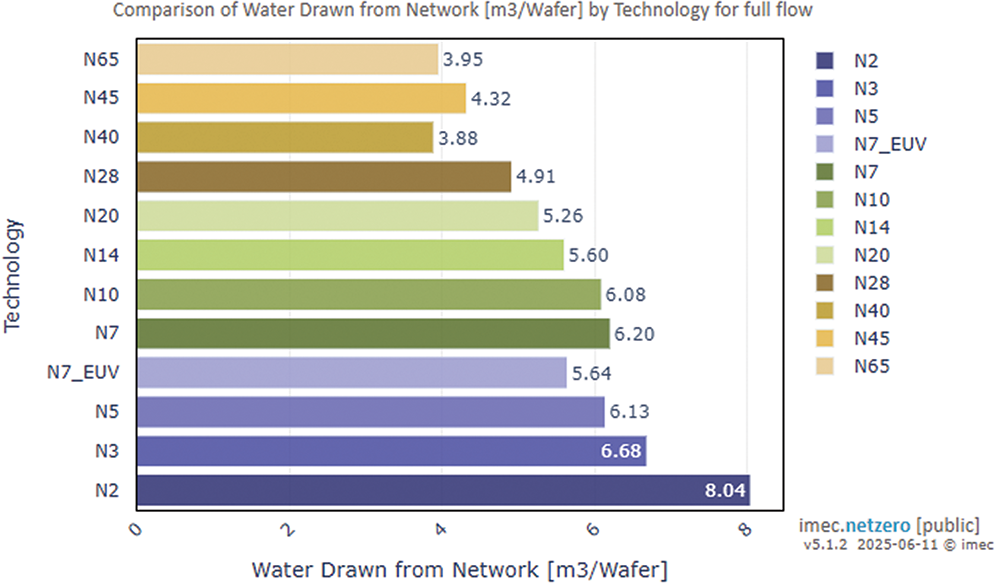
Fig. 1. Water drawn from network is projected to increase as technology node advances. Image entirely generated using imec.netzero Public (https://netzero.imec-int.com).
These external pressures, combined with growing scrutiny of environmental performance, require a clear understanding of emissions responsibilities. Emissions are typically categorized as Scope 1 (direct emissions from facility-owned sources such as fuel combustion and process gas discharges), Scope 2 (indirect emissions from purchased electricity, steam, or cooling), or Scope 3 (all other indirect emissions across the value chain, including raw materials, equipment manufacturing, logistics, and downstream impacts). Addressing all three scopes is essential for effective sustainability planning, with Scope 3 posing the greatest challenges due to its complexity and reliance on supplier data.
Sustainability is no longer an auxiliary consideration; it is becoming integral to facility planning, permitting, and long-term risk management.
Water Management Strategies
Efficient water management has become critically important as semiconductor manufacturing operations are extremely water-intensive. Several targeted strategies are recommended:
Comprehensive KPI Framework
The industry currently lacks a unified framework for evaluating sustainability comprehensively. The proposed KPI framework by the ESSF team incorporates water, energy, chemical usage, emissions, and waste management. A key feature of this approach is its sensitivity to local context. Metrics can be adjusted for water scarcity, energy mix, use of renewables (both direct and by suppliers), and discharge constraints. Early versions are being aligned with SEMI F98 to support broader industry adoption.
Technology Gaps
Several critical technology gaps have been identified:
Energy Management Practices
Strategic energy management is essential due to the complexity and interconnected nature of energy usage in semiconductor facilities. Recommended approaches include:
Scope 3 Emissions Mitigation
Indirect emissions within the value chain (Scope 3 emissions) are particularly challenging yet represent a significant sustainability opportunity. Facilities are encouraged to:
Regulatory Environment and Industry Commitments
The global regulatory landscape continues to evolve rapidly, with significant tightening of environmental regulations in key semiconductor-producing regions. Emerging regulations address emissions control, hazardous waste management, chemical restrictions (notably PFAS), and enhanced transparency requirements. Semiconductor companies have committed to ambitious environmental goals, including net-zero carbon emissions, substantial renewable energy integration, and the advancement of recycling and resource recovery methods. Early, integrated planning is essential to ensure facilities remain adaptable and compliant amid these evolving requirements.
Sustainable Equipment and Tool Design
Sustainability must be ingrained not only in facility-level management but also in the design and operation of semiconductor manufacturing tools and equipment. The roadmap highlights:
Emerging Technologies and Solutions
Emerging technologies offer promising avenues for addressing current sustainability challenges. Notable examples include:
Recommendations for Continued Development
The semiconductor industry should pursue the following strategies:
Addressing these sustainability challenges will require targeted technology development, coordinated action across the supply chain, and integration of environmental considerations into both tool and facility design. With sustained focus, the industry can reduce its environmental impact without compromising growth or innovation.
Case Study: Direct Tower Cooling for Process Cooling Water
One of the promising case studies that IRDS ESSF is working on is related to the reduction of the energy use for the manufacturing tool cooling. The explored High Temperature Process Cooling Water (HT PCW) system can potentially save an order of 10 MW of electrical energy for a typical 300 mm facility. Fig. 2 and Fig. 3 illustrate the idea.
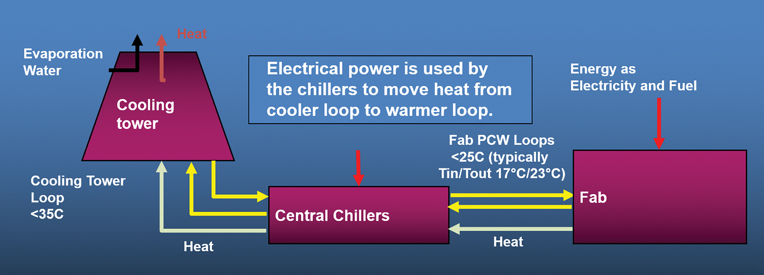
Fig. 2. Typical Fab PCW System, which have coefficients of efficiency (COEs) of 4-6 kWh/kWh.
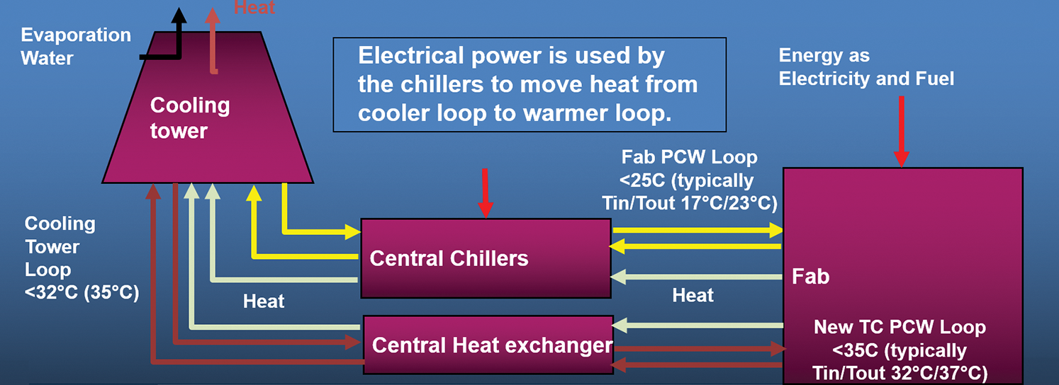
Fig. 3. Future PCW system.
The importance of this case study is due to the criticality of coordination development of such solution withing numerous industry players on both sides of the semiconductor facility technology. The manufacturing tools need to be able to operate with higher temperature PCW, whereas the support systems need to have the capability to enable effective temperature control and optimized heat recovery applications.
Your comments are most welcome. Please write directly to the Editor-in-Chief of the Newsletter at
daniel.tomaszewski@imif.lukasiewicz.gov.pl
The 9th IEEE Electron Devices Technology and Manufacturing (EDTM) Conference 2025
The 9th IEEE Electron Devices Technology and Manufacturing (EDTM 2025) Conference was successfully held in Hong Kong, China, drawing 823 participants from around the world to attend in person. Launched in 2017, the symposium was envisioned as a premier platform for researchers, engineers, and industry leaders globally to share groundbreaking discoveries, exchange ideas, and collaborate on the latest advancements in semiconductor device technology and manufacturing. Now in its ninth consecutive year, the symposium rotates locations among countries in Asia. It was previously held in Toyama, Japan (2017); Kobe, Japan (2018); Singapore (2019); Penang, Malaysia (2020); Chengdu, China (2021); Oita, Japan (2022); Seoul, Korea (2023); and Bangalore, India (2024). EDTM is rapidly establishing itself as a leading conference for the electron devices community, offering a unique forum that focuses on research and development from top universities and manufacturing companies worldwide. The symposium covers a broad range of device-related topics, including materials, processes, devices, packaging, modeling, reliability, manufacturing, and yield.

EDTM 2025 Committee Members: (left to right) Yang Chai, Tim Cheng, Mansun Chan, Yangsong Yang.
The symposium took place from Sunday to Wednesday, 9–12 March 2025, at the Hong Kong Science and Technology Park. The core members of the organizing committee for EDTM 2025 were: General Chair – Professor Yang Chai from The Hong Kong Polytechnic University; General Co-Chair – Professor Tim Cheng from The Hong Kong University of Science and Technology (HKUST); TPC Chair – Professor Mansun Chan from HKUST; and TPC Co-Chair - Professor Yansong Yang from HKUST. Unified by the theme of “Shaping the Future with Innovations in Devices and Manufacturing,” the conference featured Materials (Track 1); Process, Tools, Yield, and Manufacturing (Track 2); Advanced semiconductor (logic) devices (Track 3); Memory technologies (Track 4); Photonics, Imaging and Display (Track 5); Wide-Bandgap Power and RF devices (Track 6); Modeling and Simulation (Track 7); Reliability and testing (Track 8); Packaging and Heterogenous Integration (Track 9); Sensor, MEMS, Bio-eletronics (Track 10); Flexible and Wearable Electronics (Track 11); Nanotechnology (Track 12); and Disruptive technologies (Track 13). The symposium’s main offering comprised 4 plenary talks, 10 keynote talks, 130+ invited talks, 180 oral presentations, and 138 poster presentations. Furthermore, the program featured 9 tutorials, 12 short courses, a Women in Electron Devices & Young Professionals (WiED/YP) panel session, and an FET100 session.

EDTM 2025 Opening Ceremony.
FET100 Forum
As the Field Effect Transistor (FET) celebrates its 100th anniversary since Julius Lilienfeld’s groundbreaking 1925 patent, the IEEE Electron Devices Society (EDS) has launched a global celebration titled “100 Years of the FET” (FET100). This commemoration was inaugurated with the high-profile FET100 Forum, held as a plenary session at EDTM 2025. The forum, titled “Commemorating a Century of Field Effect Transistors and Envisioning the Next,” was hosted by Philip C.H. Chan, former Vice President of The Hong Kong Polytechnic University. It featured keynote presentations from five renowned figures in the field.
Dr. Bin Zhao, President of EDS, highlighted the FET’s century-long evolution and its fundamental role in electronics. The FET100 initiative celebrates this journey, promoting global participation and future innovation, with events and a commemorative book planned to inspire the next generation. Prof. Hiroshi Iwai from National Yang Ming Chiao Tung University detailed the FET’s evolution, focusing on Lilienfeld’s 1925 patent and the challenges in realization due to semiconductor quality and theoretical gaps. He emphasized key innovations needed for successful FET operation, including high-quality silicon and inversion channels. Prof. Chenming Hu from the University of California discussed the evolution of the BSIM compact model, highlighting its physics-based approach and open-source nature. He explored its impact on CMOS technology, multigate FETs, and quantum computing, advocating for continued openness and collaboration in modeling. Prof. H.-S. Philip Wong from Stanford University emphasized the FET’s technological, economic, and societal impact. He traced advancements in CMOS scaling, FinFETs, and nanosheets, underscoring the FET’s central role and future in domain-specific optimization. Finally, Dr. Dae-Je Chin, former President of Samsung Semiconductor, recounted Samsung’s rise in the memory industry, highlighting FET innovations and breakthroughs in DRAM development. He shared personal experiences of overcoming challenges and achieving milestones, emphasizing the FET’s pivotal role in these successes.

Plenary speakers of the FET100 session: (top row, left to right) Philip C. H. Chan, Bin Zhao, Hiroshi Iwai, (bottom row, left to right) Chenming Hu, H.-S. Philip Wong, Dae-Je Chin.
Tutorials and Short Courses
On 9 March 2025, the EDTM Tutorial/Short Course (T/SC) Program was held at Hong Kong Science Park, featuring three parallel sessions. Organized by the T/SC Committee — comprising Qiming Shao (HKUST), Tibor Grasser (TU Wien), Jianshi Tang (Tsinghua University), and Subhali Subhechha (imec) — this year’s program offered a blend of introductory tutorials and in-depth short courses led by world-renowned experts.
The tutorial sessions provided foundational insights into key emerging technologies, including AI and neuromorphic computing; 2D materials for memory, logic, and AI applications; and 3D IC technologies. Distinguished speakers from academia and industry shared their expertise. Dr. Shaodi Wang, CEO of Witmem (a leading China-based AI chip company), discussed industry trends in AI hardware development, while Prof. Max Lemme, Director of AMO GmbH (a German nanotechnology research institute) and Professor at RWTH Aachen University, presented advancements in fab-compatible 2D material processing.

A scene from the Tutorial/Short Course.
The short course program covered specialized topics such as quantum technology (co-organized by the IEEE EDS Emerging Technology Technical Group), emerging computing and sensing systems, and wide bandgap semiconductors. Esteemed speakers included Prof. Srabanti Chowdhury (Stanford University) and Prof. Kevin Chen, who delivered comprehensive talks on GaN vertical devices and power integration, respectively. Dr. Peter Moens (onsemi, an American semiconductor supplier company) provided an industry perspective on SiC power MOSFET technology and reliability.

Prof. John Paul Strachan presenting the keynote speech at the MT session.
Technical Tracks Highlights
The Advanced Semiconductor Devices track featured 4 parallel sessions and a poster session, with 10 invited talks, 14 oral talks, and 12 posters. Topics included Si/Ge devices, CMOS scaling, oxide and 2D semiconductor devices, and 3D integration. Highlights included Prof. Yunlong Li’s insights on CMOS pilot lines, discussions on reliability and applications of oxide and 2D devices, and advancements in 3D integration by Prof. Yuan Liu, Prof. Saptarshi Das, Prof. Sanghyeon Kim, and Prof. Heng Wu. The sessions explored innovations in high-density 3D integration, heterogeneous 3D CFETs, and beyond conventional 3D integration, with additional talks on tunnel FETs and Ge FinFET CMOS inverters.
The Memory Technology (MT) track at EDTM 2025 was a standout, attracting the most submissions with 87 papers, highlighting the dynamic nature of memory research. The program featured 13 invited talks, 28 oral presentations, and 24 posters, covering advancements in DRAM, Flash, and emerging non-volatile memories like RRAM, ferroelectric RAM, MRAM, and phase-change memory. Innovations focused on faster data transfer, lower power consumption, and enhanced durability. The track also explored novel 3D structures, high-density integration, and applications in in-memory and neuromorphic computing, emphasizing memory’s expanding role. With speakers from global institutions, the sessions fostered discussions on performance metrics and challenges, establishing the MT track as a key forum for advancing next-generation electronics. Participants addressed challenges like thermal management, endurance limitations, and future scaling roadmaps.
The Modelling and Simulation Track at EDTM 2025 featured keynote speeches, technical presentations, and interactive poster sessions, attracting 66 attendees from diverse regions. With 59 accepted papers, the program covered topics like compact modeling, emerging device simulations, and machine learning models. Keynote speaker Prof. Tibor Grasser discussed gate dielectrics for 2D electronics. Networking events, including a banquet and gatherings, fostered collaboration and discussions among participants, enhancing connections and advancing research in electronic device modeling and simulation.

Attendees of the WiED/YP Panel Session.
Special Events
The IEEE EDS 2025 WiED/YP Panel Session, themed “Empowering Innovators,” was held at the IEEE EDTM Conference in Hong Kong. Chaired by Prof. Pei-Wen Li, the session featured panelists Dr. Lydia Leung, Prof. Wei Liu, and Prof. Suting Han, who shared insights on professional growth, work-life integration, and overcoming career challenges. Sponsored by IEEE EDS, the event attracted 25 participants and emphasized empowering women and young professionals in electronics. The session concluded with a group photo, highlighting the spirit of collaboration and innovation.
The IEEE EDS hosted a Rump Session on neuromorphic computing at EDTM 2025, featuring insights from five panelists on materials, architectures, algorithms, reliability, and commercialization. Attended by 170 participants, the session explored challenges and opportunities in transitioning neuromorphic computing from research to real-world applications. Discussions emphasized overcoming reliability and manufacturability hurdles, integrating analog and digital approaches, and fostering collaboration between academia, industry, and government. The event highlighted the commitment to advancing electronics and semiconductor research and interdisciplinary innovation.

Speakers of the Rump Session on neuromorphic computing.

Dr. Bin Zhao presenting the Simon Sze Education Award to Professor Mohamed Jamal Deen.
Simon Sze Education Award
At EDTM 2025, the IEEE EDS celebrated the renaming of the EDS Education Award to the Simon Sze Education Award, honoring Professor Simon Sze’s contributions to semiconductor education. The ceremony featured speeches by Dr. Bin Zhao, Dr. Nicky Lu, and Professor Hiroshi Iwai, highlighting Sze’s legacy and the Award’s significance. Dr. Lu shared personal memories of Sze’s teaching impact, while Professor Iwai detailed the Award’s history and Sze’s influential textbook, Physics of Semiconductor Devices. The inaugural award was presented to Professor Mohamed Jamal Deen “for impactful leadership and global dissemination of biosensor education in underprivileged regions.” Deen emphasized storytelling in teaching and his support for female researchers. The event recognized contributions from IEEE Foundation members and NYCU representatives, celebrating Sze’s lasting influence on the semiconductor field.
Celebration of Contributions and Friendships
The social highlight of the Symposium was none other than the welcome banquet with local characteristics of Hong Kong on Tuesday evening. There were plenty of reasons to celebrate—incredible progress in our industry, all-time high paper submissions, a record attendance onsite after 9 years, and the in-person experience in Hong Kong to reconnect with old friends and meet new ones. Heartfelt thanks to the organizing committee, technical program committee, sponsors, and volunteers whose tireless efforts have made IEEE EDTM 2025 possible. Your dedication and commitment have been instrumental in shaping this event into a world-class conference. We also want to thank our attendees, speakers, and exhibitors for your contributions and participation. Your presence enriches the conference and ensures its success.

Participants enjoying entertainment in Hong Kong.
The EDTM Symposium returns to Penang, Malaysia, from Sunday to Wednesday, 1-4 March 2026. For the latest updates, please visit https://ewh.ieee.org/conf/edtm/. We look forward to seeing you again next year!
Yang Chai, General Chair of EDTM 2025
2025 IEEE International Memory Workshop (IMW) |
The 17th International Memory Workshop (IMW) took place at the Portola Hotel & Spa in Monterey, California, on 18–21 May 2025. This year, organizers elected to hold the event at a new venue in Monterey, which was located within the city center and provided easy access to the city’s beautiful scenery, nightlife, and attractions.
IMW is sponsored by the IEEE Electron Devices Society and meets annually in May. The workshop is a unique forum for specialists in all aspects of semiconductor memories (non-volatile and volatile). The scope of the workshop content ranges from new memory concepts in early research to the technology drivers currently in volume production, as well as emerging technologies in development. The technical sessions are organized in a manner that provides ample time for informal discussions amongst presenters and attendees.

The Organizing Committee of IMW 2025 opening the conference.
The event began with a one-day short course consisting of two tutorial sessions, “Advanced DRAM and High Bandwidth Memories” in the morning and “Emerging Memories” in the afternoon. The technical program for the single-track conference spanned three days and opened with a keynote session featuring talks by Krishnan Subramanian of Micron who presented “NAND Flash Innovation in the AI Era,” Su Jin Ahn of Samsung who presented “Future Technology Outlook on DRAM/Flash Memories for More Moore and More Than Moore,” and Dmitri Strukov of the University of California, Santa Barbara who presented “Controlling ReRAM’s Switching Characteristics with Shadow Memory for Continual Learning.” The program continued with additional sessions dedicated to DRAM, Emerging Memories, Ferroelectric Memories, in-memory computing, and NAND.
Many sessions held invited talks given by experts in the memory field: Onur Mutlu of ETH Zurich presented “Memory-Centric Computing: Solving Computing’s Memory Problem;” Steven Lemke of SST presented “Reliability and Accuracy of a Qualified Split-Gate Flash In-Memory Compute Technology;” Sidney Tsai of IBM presented “Analog AI Accelerators for Transformer-based Language Models: Hardware, Workload, and Power Performance;” Syed M. Alam of Everspin presented “STT-MRAM Antifuse Macro for Memory, SoC, and FPGA Chips;” and Asif Khan of Georgia Tech presented “Ferroelectrics for Vertical NAND Flash Applications.”
As reflected in the keynote presentations and invited talks, it is clear that the main focus within the industry centers around the challenges posed by AI applications. This topic, along with varying perspectives, was incorporated into a very interesting panel session led by Jian Chen of Micron. Distinguished panelists included Insoo Yoon of Sandisk, Seho Lee of SK Hynix, Sidney Tsai of IBM and Anand Joshi of TechInsight.
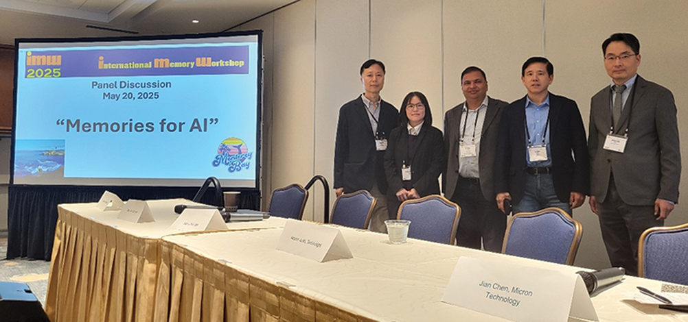
Panel Discussion on “Memories for AI”.
The IMW is an excellent forum to present new and original technical works. This year’s technical program received more than 70 submissions and adhered to a superior acceptance rate of 25–45%, thus aiming for the highest quality program. Thirty-three papers were accepted, which included 18 oral presentations and 15 posters covering the major categories of memory technologies (NAND, DRAM, Ferroelectric, SOT, RRAM, SRAM, PCM and selectors) and NVM applications (Automotive, In-memory and Neuromorphic Computing).
Two papers were selected by the Technical Committee for the annual Best Paper Awards. Hiroshi Maejima from Kioxia received the Best Paper Award with his contribution titled “Crossed Bit Line Architecture (CBL) in 3D Flash Memory CMOS Directly Bonded to Array (CBA) Structure.” The Best Student Paper Award was presented to Mor Dahan from Technion Israel Institute of Technology, with the paper titled “Novel Ultrafast Non-Destructive Readout of FeRAM by Low-Voltage Transient Current.”
Traditionally, IMW achieves a large participation when held in Asia. This year, organizers were pleased to see a 35% increase in attendance from the last time it was held in Monterey (2023). With more than 200 attendees who traveled from many different parts of the world, the largest hailed from the USA, with 50% representation, followed by Asia at 38% and Europe at 11%. To help promote increased networking and the exchange of ideas amongst attendees, organizers, speakers and sponsors, multiple social activities such as breakfasts, coffee breaks, lunches and evening socials were incorporated into the registration fee. This, along with a casual dress code and support from our industry partners, aided in delivering a cohesive, high-quality workshop experience.

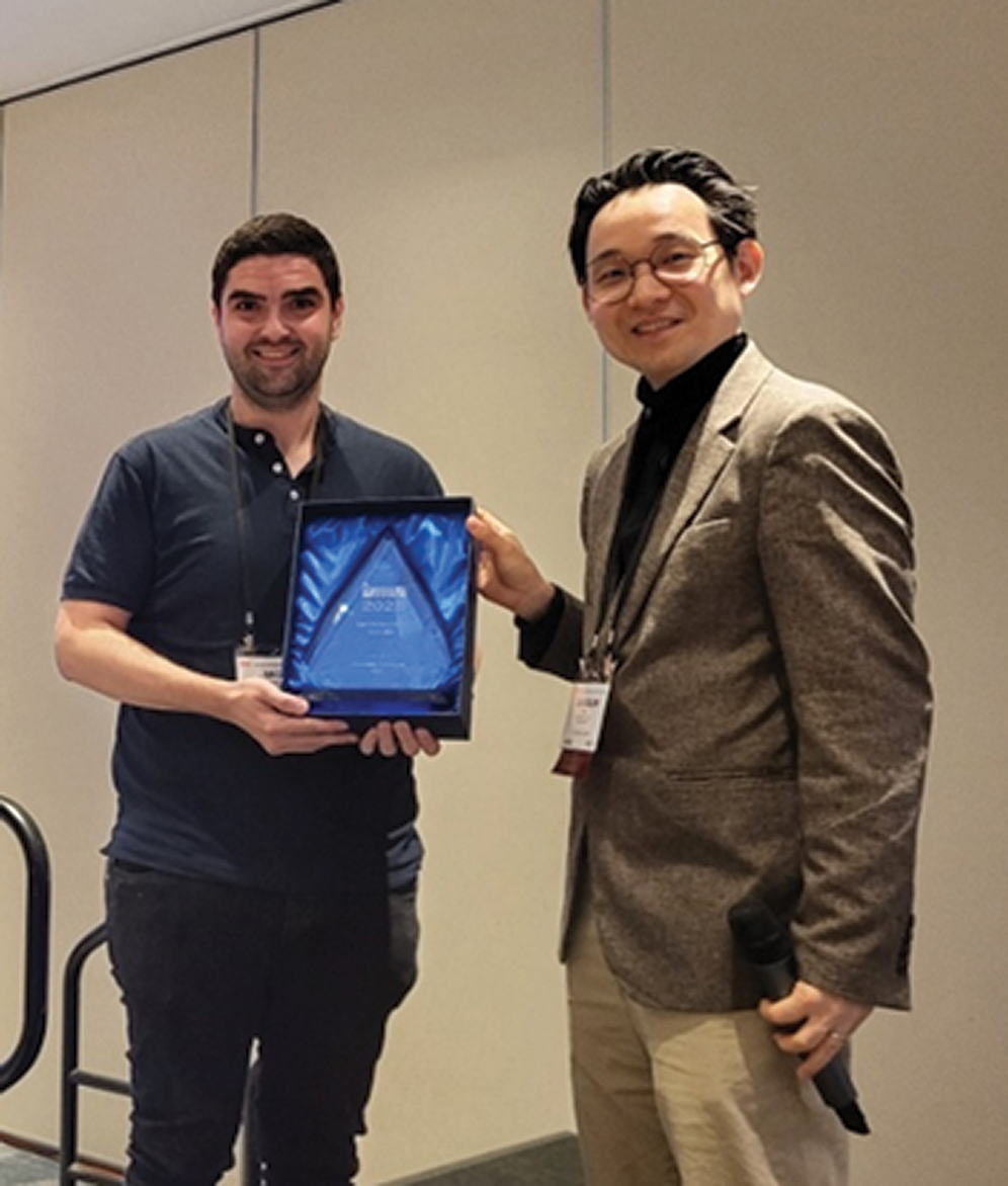
2025 Best Paper recipient Hiroshi Maejima (on left).
2025 Best Student Paper recipient Mor Dahan (on left).
Technical proceedings from all editions of the IEEE International Memory Workshop (IMW) can be found on the IEEE Xplore® platform at: https://ieeexplore.ieee.org/xpl/conhome/
1002800/all-proceedings.
Finally, organizers are pleased to announce that the 2026 IMW will be held 10-13 May in Leuven, Belgium. For more details, please visit the website: http://www.ewh.ieee.org/soc/eds/
imw/.
Antonio Arreghini
2025 IEEE IMW Publicity Chair