Technical Briefs
Micro-Transfer Printing
Technology Enables
Heterogeneous Integration
for 3D ICs
3D heterogeneous integration of many diverse ultra-thin components improves the power, performance, area, cost, time-to-market, and security of high-performance computing, communications, mobile, automotive, industrial, medical, and defense systems. These diverse components include high electron mobility transistors (HEMTs), heterojunction bipolar transistors (HBTs), power transistors, gate drivers, photonics, sensors, hardware assurance devices, capacitors, inductors, filters, and antennas manufactured using many different process nodes and technologies, including SOI, GaAs, GaN, InP, and SiGe.
Micro-transfer printing (MTP) technology, a patented process developed by X-Celeprint, employs a massively parallel pick-and-place process to stack large arrays of ultra-thin (1—20 micron) diverse components, called x-chips, from one or more separately manufactured wafers on a variety of destination substrates to improve heterogeneous integration to create a 3D IC with the following improvements in:
MTP technology supplements other conventional and advanced packaging technologies, providing 3D IC manufacturers with a unique “tool-in-the-toolbox” optimized for heterogeneous integration of large arrays of ultra-thin, diverse components. An MTP-based 3D IC (Figure 1) is manufactured using the following steps: 1) Source wafer fabrication; 2) Destination wafer or substrate fabrication; 3) MTP stamp fabrication; 4) MTP pick-and-place; and 5) Thin film interconnects.
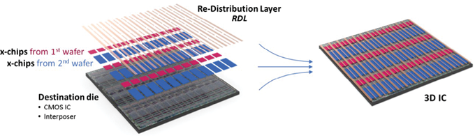
Figure 1. 3D IC made with MTP Technology.
1) Source Wafer
Tightly packed x-chips are fabricated on source wafers made using the optimal process node and technology (such as SOI, GaN, GaAs, InP and SiGe) for each component. A sacrificial layer is formed underneath the x-chips using different techniques depending upon the source wafer technology, such as:
A tether/anchor system (Figures 2 and 3) holds the x-chips aloft after the source wafer is anisotropically etched to remove the sacrificial layer everywhere but underneath the anchor.
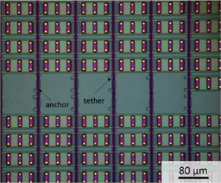
Figure 2. X-chips on source wafer after partial x-chip pick-up.
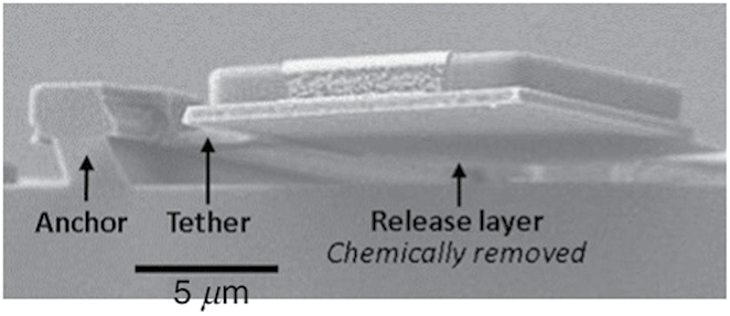
Figure 3. X-chip after chemical etch.
2) Destination Substrate
There are many options for the destination substrate, including silicon wafers with integrated CMOS ICs, silicon, glass, or ceramic interposer wafers, and large-area glass, ceramic, or plastic panels. The substrate’s surface may be planar or non-planar and be smooth or rough.
3) MTP Stamp Fabrication
A low-cost, reusable mold is used to make the MTP stamp (Figure 4) which consists of an array of soft posts composed of a compliant elastomer material, polydimethylsiloxane (PDMS), on a stiff glass substrate. The stamp is stiff in the x-y dimensions, providing high placement accuracy, and compliant in the z-dimension, accommodating non-planar and rough destination substrates. The post array on the stamp (Figure 5) is customized to match the desired destination substrate locations for massively parallel, selective pick-and-place of thousands of x-chips.
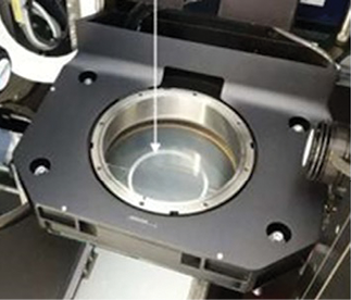
Figure 4. MTP stamp.
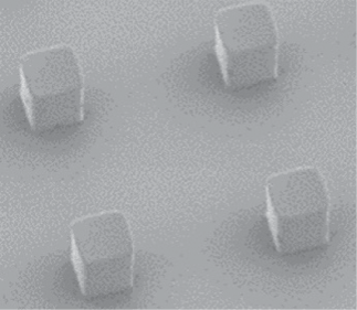
Figure 5. Close-up of MTP stamp’s posts.
The stamp’s posts adhere to the x-chips via van der Waals force. The stamp’s viscoelastic behavior uses fast separation speed during pick-up to break the tethers and remove the x-chips, and slow separation speed to place the x-chips on the destination substrate. Using a “step and repeat” process, the entire destination substrate is populated with x-chips. The stamp can pick-and-place x-chips from smaller to larger wafers (Figure 6) with high wafer utilization, as the stamp readily handles x-chips at the wafer’s edge.
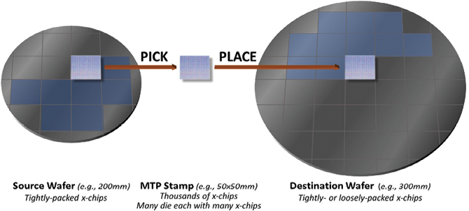
Figure 6. Transfer from smaller source wafer to larger destination wafer.
The x-chips may be transferred from multiple source wafers to different locations within the same die on the destination wafer to combine components made using multiple process technologies (Figure 7). By adjusting the pattern and spacing of the small posts on the transfer stamp, the x-chips may be tightly-packed on the source wafer, reducing cost via high wafer utilization, and either tightly- or loosely-packed on the destination wafer.
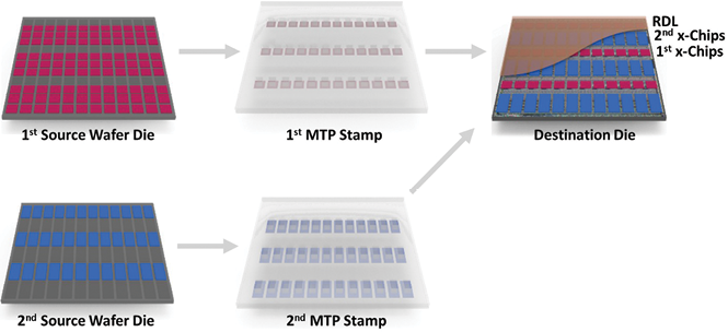
Figure 7. Single die close-up of transfer from two source wafers to a destination wafer.
4) MTP Pick-and-Place
An ultra-high precision pick and place tool developed by AMS Amicra is used to implement MTP technology via a high throughput, fully automatic ISO clean room class 10 system employing a 50 × 50 mm MTP stamp for massively parallel pick-and-place of x-chips from source wafers, which can be up to 300 mm, to destination substrates, which can be up to 300 mm wafers or 450 × 450 mm panels. Placement accuracy is plus-or-minus 1.5-microns with a 40 second cycle time. Other implementations of the MTP technology include systems with higher placement accuracy (plus-or-minus 0.5-micron) and a low-volume system to serve R&D and specialized manufacturing markets.
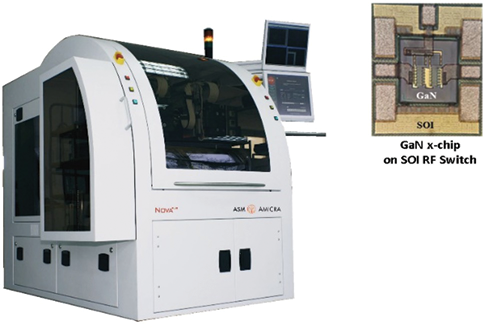
Figure 8. High volume MTP manufacturing system developed by AMS Amicra; for details of inset see Fig. 12 caption.
5) Thin Film Interconnects
Since the x-chips are ultra-thin (1—20 micron), thin film interconnects may be readily used to connect the x-chips and destination die, resulting in very short path lengths, since both are active side up. Figures 9 and 10 show the top and cross section views of x-chips interconnected with a copper redistribution layer (RDL). The RDL provides a low electrical and thermal resistance path and enables use of multiple conventional and advanced packaging options.
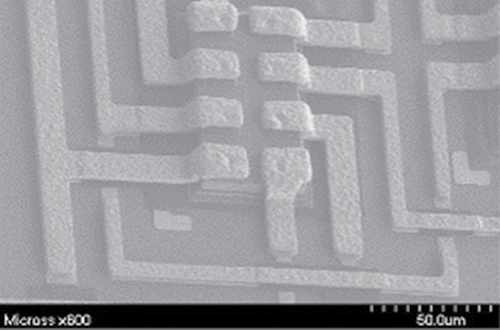
Figure 9. X-chip with RDL top view.
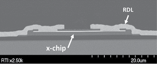
Figure 10. X-chip with RDL cross-section view.
Examples
Figures 11–16 show a wide variety of prototypes manufactured using MTP:
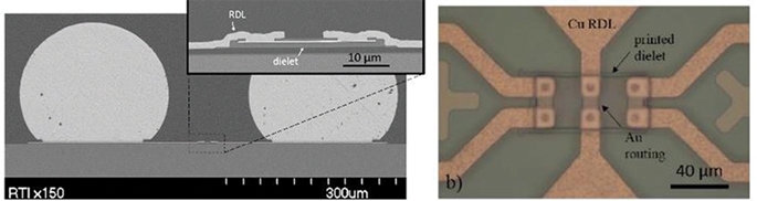
Figure 11. Fan-Out Packaging of Microdevices Assembled Using Micro-Transfer Printing (https://doi.org/10.1109/ECTC.2016.269).
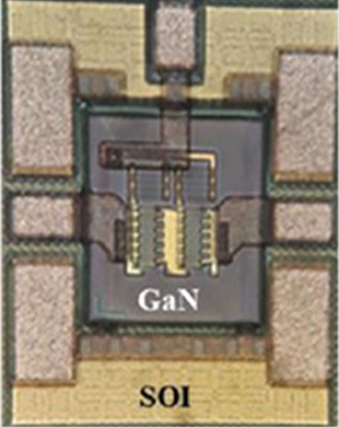
Figure 12. Drillet, F., Loraine, J., Saleh, H., . . . U’Ren, G. (2021). RF Small and large signal characterization of a 3D integrated GaN/RF-SOI SPST switch. Int. J. Microwave and Wireless Technol., 13(6), 517-522. doi:10.1017/S1759078721000076.
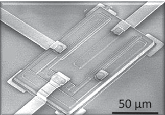
Figure 13. Integration of GaN HEMTs onto Silicon CMOS by Micro Transfer Printing (https://doi.org/10.1109/ISPSD.2016.7520875).
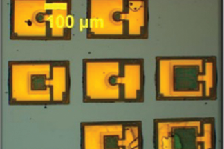
Figure 14. Mathews, I., Quinn, D., Justice, J., . . . Corbett, B., Microtransfer Printing High-Efficiency GaAs Photovoltaic Cells onto Silicon for Wireless Power Applications. Adv. Mater. Technol. 2020, 5, 2000048. https://doi.org/10.1002/admt.202000048. Copyright Wiley-VCH GmbH. Reproduced with permission.
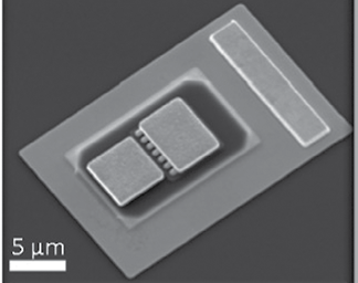
Figure 15. Microtransfer-Printed InGaAs/InP HBTs Utilizing a Vertical Metal Sub-Collector Contact (https://doi.org/10.1109/DRC46940.2019.9046426).
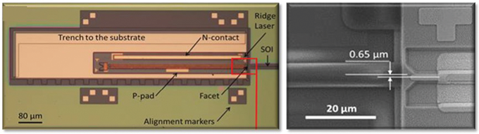
Figure 16. Edge-coupling of O-band InP etched-facet lasers to polymer waveguides on SOI by micro-transfer-printing (https://doi.org/10.1109/JQE.2019.2958365).
About the Authors

Bob Conner is VP of Business Development at X-Celeprint. Previously, he was CEO of Sarda Technologies and Symmorphix. Bob has held VP positions at Semprius, Nextreme, and Cirrus Logic and worked for Applied Materials, Intel, and GE. Bob earned his MBA at University of Chicago and BSME at Duke University.

Dr. Johann Weinhändler is Managing Director at ASM AMICRA. Previously, he has held different management positions at Oerlikon Systems, Datacon/Besi, and Lam Research.
Johann earned his Ph.D at the Trinity Colleges Dublin and an MBA from the Open University Business School in the UK.
Your comments are most welcome. Please write directly to the Editor-in-Chief of the Newsletter at daniel.tomaszewski@imif.lukasiewicz.gov.pl