75th Anniversary
of the Transistor
History of Naming Non-planar
FET Devices
By Digh Hisamoto
Today, with the advent of FinFET, the mainstream of advanced devices has evolved from conventional planar to non-planar structures. Historically, fin devices have paved the way for the development of practical double-gate FET (field-effect transistor) by combining two separate approaches: the study of double-gate mechanisms and non-planar channel structures. The name FinFET is the current industry-standard terminology, but many other names were proposed in the past. I would like to take a bird’s-eye view of the history of developing non-planar devices by tracing their names. The narrative is based partly on my own involvement and partly on my understanding of device evolution gathered from numerous patents and papers that I have collected. In some cases, the exact time frames of various inventions might not be precise, but the overall sequence of events should be fairly accurate. First, let us look back on the history of double-gate mechanisms research before the birth of the fin structure.
The first description of a double-gate structure appeared in a patent by Oskar Heil [1]. He is known as the inventor of the FET after Julius Edgar Lilienfeld developed the field effect concept in an earlier patent [2]. A structure in which a thin semiconductor layer is sandwiched between upper and lower gate electrodes is depicted in Heil’s patent. It is remarkable that this patent, which was derived from the image of capacitor elements, described the effect of reducing the thicknesses of the gate-insulating film and the semiconductor layer. At that time, the word “transistor” did not even exist, and there is no evidence that the device was given a name.
In the 1960s and 1970s, after the invention of various transistors including metal-oxide-semiconductor FETs (MOSFETs), double-gate structures were actively analyzed, and most of the basic ideas still in use today were explored. The term 4-terminal also seems to have been used after the Junction Field Effect Transistor (JFET) along with the double-gate FET [3], [4]. Experimentally, the device structure was realized by depositing multiple thin films on the substrate. Therefore, it seems that it was generally recognized as a thin-film transistor (TFT) [5]. Various semiconductor materials such as amorphous silicon, Cadmium Sulfide, Cadmium Selenide, and Tellurium were studied as semiconductors for the channel. This situation changed significantly around 1980 when the technology for manufacturing Silicon on Insulator (SOI) substrates using ion implantation technology (separation by implanted oxygen: SIMOX) was developed, and SOI devices with silicon single-crystal channels were produced [6]. Although the ideal channel sandwiched by the gates that have been analyzed could not be fabricated, the supporting substrate could be used as a pseudo-gate electrode. Using this approach, the characteristics of double-gate devices with single-crystal semiconductor channels have been experimentally demonstrated [7]. At that time, the term “thin-film SOI” was often used. In the early stages of research using SOI, the name X-MOS was proposed by Toshihiro Sekigawa and Yutaka Hayashi because the shape sandwiched between the gates resembled the Greek capital letter Ξ, corresponding to the letter “X” [8]. Although the name was mentioned in many references, there is no evidence of its widespread use because the structure itself has been widely known for a long time.
Next, looking at research on non-planar channel structures, this field made great progress with the establishment of silicon-substrate etching technology in the second half of the 1960s. It seems that power devices have driven the evolution of non-planar devices rather than large-scale integration (LSI) devices, which have improved the degree of integration through device scaling. It was first formed using the crystal orientation dependence of wet etching, and later dry etching by reactive ion etching was used. Devices fabricated by wet etching are called V-MOS or V-groove MOS due to the characteristic channel shape [9]. To increase the trench density and avoid electric-field concentration at the tip of the V-groove, rectangular trenches were first formed by skillfully using the crystal orientation dependence of wet etching [10]. After that, due to advances in etching technology and interfacial treatment technology, the grooves were formed by dry etching [11]. These are commonly called U-MOS due to their rounded trench-bottom shape [12]. Since UMOS demonstrated that the sides of trenches made perpendicular to the substrate surface can be used as channels, many structures using the sides as channels were proposed in the 1970s and 1980s. The name trench MOS or trench-gate was often used. Power devices require high current-driving capability per unit area, so trench structures were attracting attention as a way to expand the channel width. Initially, there was only one trench, but in order to increase the number of sides, it was considered better to form multiple trenches side by side [13]. By thinning the walls between the trenches, the structure evolved into one consisting of gates from both sides [14], [15]. These structures were also considered as trench MOS and there is no evidence of a different name. However, this idea led to laterally diffused MOS (LDMOS), also known as lateral trench-gate or folded-gate LDMOS [16].
Looking at LSI devices, device scaling progressed in the 1970s, and the short-channel effect became increasingly important. To increase the effective channel length or increase the channel width even if the channel length is the same, the use of trenches was considered as an extension of the planar structure. Those with longer channel lengths are often called grooved-gates, and those with wider channel widths are often referred to as trench gates or folded channels. It has become clear that the trench structure poses serious problems considering LSI devices rather than power devices. Regarding LSI devices supported by planar processing technology, topologically speaking, a trench gate basically has a channel outside the gate. Therefore, when integrating devices, so-called isolation problems such as interference with adjacent devices arise. For example, even if several trenches are arranged in parallel, there will inevitably be a structure that cannot be covered with gates at the outermost periphery or at the bottom of the device. It was clear that integrating multiple devices would cause interference between devices. For this reason, though trench gates were first proposed in the LSI field, pillar gates, in which the gate covers the channel, were later considered. I surmise that this is one of the reasons why Hitoshi Takato and his colleagues named the first pillar-shaped device in LSI the surround gate transistor (SGT) [17]. There was still work to be done to knock down the pillars as with the lateral groove structure, but these studies have set the stage for the emergence of the fin structure.
In the latter half of the 1980s, my collaborators at Hitachi and I developed the first fin-type device on the basis of the idea of making fins by knocking down pillars or thin walls and name it a fully depleted lean-channel transistor or DELTA, imagining the δ-function [18]. I decided on this name because I thought that in addition to the similarity in shape, it would also highlight the fact that it can be isolated from adjacent devices for LSI. I also used the word “lean” to describe the feature, borrowed from the field of chemistry, where it is a common term that means low concentrations in gases and liquids and used, for example, in lean combustion. Therefore, I decided to adopt the term for the solid phase, although it might have been misused. At that time, the necessity of lowering the channel concentration for device scaling was not widely recognized, so the device name DELTA was adopted to emphasize the necessity of reducing the impurity concentration of the substrate (channel). However, the word DELTA has a stronger image of a triangle than the δ-function, and was not associated with the shape of the device. As a result, the name DELTA did not become very popular.
In the late 1990s, I collaborated with Device Group at UC Berkeley, directed by Professors Jeffrey Bokor, Tsu-Jae King, and Chenming Hu, to demonstrate further miniaturization using fin structures. At that time, we decided to use the name folded-channel for the device from discussions at the group meetings. I have noticed that the thickness of the gate-stack structure becomes a challenge when applying device scaling to the fin structure.
As shown in Fig. 1, the gate is arranged to cover the channel in the fin-type device. Even in DELTA, the first fin-type to use the quarter-micron technology, we can see the gate occupying a large part of the device. Considering the generation with a channel length of 20 nm or less, the fin thickness, gate insulating film thickness, and gate electrode thickness can be expected to be tf≃10 nm, tox≃5 nm, and tg≃20 nm, respectively. In this case, the total width will be 60 nm, which is the sum of the width of the fin and twice the thickness of the gate stack on either side of the fin. This is, of course, much larger than the channel length, and I expected the time would come when device scalability would be dominated by the gate-stack thickness. Therefore, the word “fold”, which means bending the gate electrode, carries an important message, so I thought it was not a bad name.
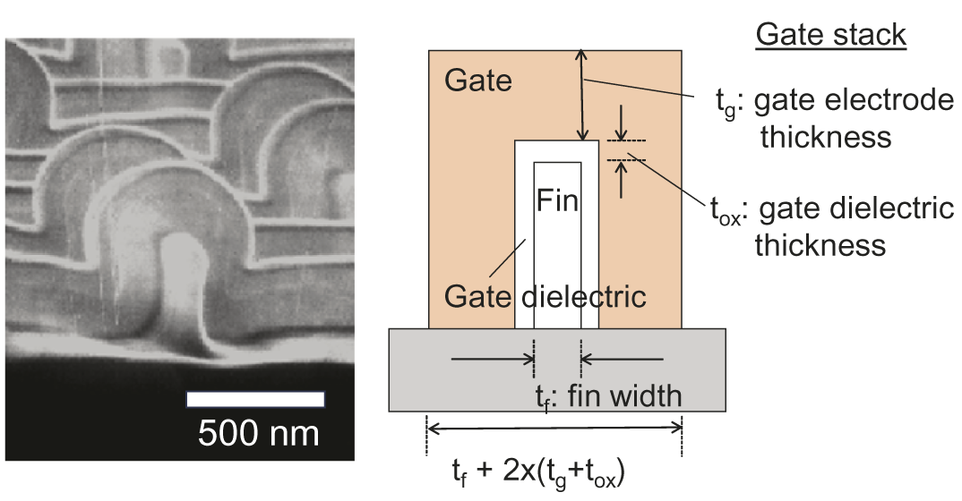
Figure 1. SEM image of the first fin device DELTA (left) and the size of the fin device configuration (right). In the scaled fin-type device, it can be seen that the gate stack structure occupies most of the device.
I presented this folded-channel structure at the 1998 IEDM (International Electron Devices Meeting) held in San Francisco [19]. The following year, when we were preparing to submit a manuscript to the IEDM, I was asked by Professor Hu about the name. According to him, at a conference he attended, he heard someone calling the channel of our device a fin and thought about calling it FinFET. I remember agreeing immediately. This is because the moment I heard the word fin, the word Fin that appears in the end roll of French movies that I often watched as a child under the influence of my mother came to my mind, and I thought that this would signify the last FET. Before this, the source-channel-drain structure was sometimes called fin in the Japanese semiconductor community, as it resembles the fins of a fish. However, since it was not alphabetic, it had never occurred to me that fin could be connected to the meaning of “the last”. Thus, I told the editor who was in charge of the paper I had already submitted that I wanted to change the device name and the title used in the manuscript, and was able to obtain the editor’s approval [20]. At the 1999 IEDM held in Washington, D.C. in December, we reported the device structure for the first time under the name FinFET [21].
These presentations prompted many universities, research institutes, and companies to publish research on FinFET in conferences and journals. Most used the name FinFET, but some used names such as π-gate or Ω-gate [22], [23]. I think the use of Greek letters for these names was a tribute to the name DELTA used in the initial announcement, and I am grateful to them.
At the 2002 SSDM (International Conference on Solid State Devices and Materials), Robert Chau and colleagues of Intel made the first conference presentation using the tri-gate name [24]. I presumed that the reason for using tri-gate instead of FinFET was to show that it was an improvement over the double gate. This naming led to the movement to classify non-planar devices by the number of gates surrounding the channel. They are classified into single gates, double gates, triple (tri) gates, and quadruple gates, and are collectively called multi-gates or MUGFETs. However, I felt a little uncomfortable with this classification and naming. The reason is that the principle of operation is the same even if there are multiple gate electrodes, so I thought it would be more appropriate to use the same terminology. As FinFET evolution proceeded by scaling the fins taller and narrower, resulting in a more fin-like shape, these names fell out of use and converged on FinFET. It became widely accepted because the shape can be easily visualized, thus appropriate. I believe that this naming has had a great effect in revitalizing and advancing device research.
Gate-all-around (GAA) has been mentioned as the next-generation non-planar structure after the current FinFET. GAA is a long-time name proposed by Jean-Pierre Colinge and his colleagues the year after DELTA was announced [25]. For some time, the name nanowire was more popular than GAA, but it faded due to problems with the driving current. After that, names such as multi-bridge, nano-sheet, and nano-ribbon have appeared. Currently, GAA seems to be the most commonly used, though the layered structure of the channel is not well described by this name. It is my fervent hope that a more descriptive name will emerge in the near future for the next non-planar FET structure.
At the end of the article, the author would like to thank Dr. Eiji Takeda, Prof. Chenming Hu, Dr. Samar Saha, Prof. Manoj Saxena, and Dr. Daniel Tomaszewski for their valuable support and suggestions regarding the writing of this article.
References
[1] O. Heil, British Patent 43947 (filed in 1935, issued in 1935).
[2] J. E. Lilienfeld, US Patent 1745175 (filed in 1925, issued in 1930).
[3] S. S. Perlman, and K. H. Ludewig, “An Adaptive Thin-Film Transistor,” IEEE Trans. Electron Devices, Vol. ED-14, no. 12, pp. 816-821, 1967.
[4] P. K. Weimer, “The TFT—A New Thin-Film Transistor,” Proc. IRE, Vol. ED-14, no. 2, pp. 69-74, 1967.
[5] H. R. Farrah, and R. F. Steinberg, “Analysis of Double-Gate Thin-Film Transistor,” IEEE Trans. Electron Devices, Vol. ED-14, no. 2, pp. 69-74, 1967.
[6] E. Sano, et al., “A Two-Dimensional Analysis for MOSFET’s Fabricated on Buried SiO2 Layer,” IEEE Trans. Electron Devices, Vol. ED-27, no. 11, pp. 2043-2050, 1980.
[7] J. P. Colinge, “Subthreshold Slope of Thin-Film SOI MOSFET’s,” IEEE Electron Device Letters, vol. 7, no. 4, pp. 244-246, 1986.
[8] T. Sekigawa, and Y. Hayashi, “Calculated threshold-voltage characteristics of an XMOS transistor having an additional bottom gate,” Solid-State Electronics, Vol. 27, nos. 8/9, pp. 827-828, 1984.
[9] F. E. Holmes, and C. A. T. Salama, “V groove M.O.S. transistor technology,” Electronics Letters, vol. 9, pp. 457-458, 1973.
[10] E. S. Ammar, and T. Rodgers, “UMOS Transistors on (110) Silicon,” IEEE Trans. Electron Devices, vol. ED-27, no. 5, pp. 907-914, 1980.
[11] D. Ueda, et al., “A New Vertical Sidewall Channel Power MOSFET with Rectangular Grooves,” Extended Abstracts, International Conference on Solid State Devices and Materials, pp. 313-316, 1984.
[12] D. A. Smith, and C. A. T. Salama, “A UMOS power field effect transistor,” Solid-State Electronics, vol. 23, no. 6, pp. 687-692, 1980.
[13] T. Masuhara, et al., Japanese Unexamined Patent Application Publication No. 1975-8483, filed on May 21, 1973.
[14] K. Hirashima, et al., Japanese Unexamined Patent Application Publication No. 1979-99573, filed on January 24, 1978.
[15] Y. Hayashi, Japanese Unexamined Patent Application Publication No. 1982-10973, filed on June 24, 1980, (later Japanese Patent No. 1791730, issued on October 14, 1993).
[16] Y. Kawaguchi, et al., “20 V and 8 V Lateral Trench Gate Power MOSFETs with Record-Low On-resistance,” Tech. Dig., IEDM, pp.197-200, 1999.
[17] H. Takato, et al., “High Performance CMOS Surrounding Gate Transistor (SGT) for Ultra High Density LSIs,” Tech. Dig., IEDM, pp. 222-225, 1988.
[18] D. Hisamoto, et al., “A fully depleted lean-channel transistor (DELTA)— a novel vertical ultra thin SOI MOSFET,” Tech. Dig. IEDM, pp. 833-836, 1989.
[19] D. Hisamoto, et al., “A folded-channel MOSFET for deep-sub-tenth micron era,” Tech. Dig. IEDM, pp. 1032-1034, 1998.
[20] D. Hisamoto, et al., “FinFET–a self-aligned duble-gate MOSFET scalable to 20 nm,” IEEE Trans. Electron Devices, vol. 47, pp. 2320-2325, 2000.
[21] X. Huang, et al., “Sub 50-nm FinFET: PMOS,” Tech. Dig., IEDM, pp. 67-70, 1999.
[22] J.-T. Park, et al., “Pi-gate SOI MOSFET,” IEEE Electron Device Letters, vol. 22, no. 8, pp. 405-406, 2001.
[23] F.-L. Yang, et al., “25 nm CMOS Omega FETs,” Tech. Dig., IEDM, pp. 255-258, 2002.
[24] R. Chau, et al., “Advanced Depleted-Substrate Transistor: Single-gate, Double-gate, and Tri-gate,” Extended Abstracts, International Conference on Solid State Devices and Materials, pp. 68-69, 2002.
[25] J. P. Colinge, et al., “Silicon-on-insulator ‘gate-all-around device’,” Tech. Dig., IEDM pp. 595-598, 1990.
Biography
 Digh Hisamoto received the B.S., M.S., and Ph.D. degrees from the University of Tokyo in 1984, 1986, and 2003, respectively. In 1986, he joined Central Research Laboratory, Hitachi, Ltd., Tokyo, where he has been working on ULSI device physics and process technologies. He developed scaled CMOS and memory devices including DELTA, the original model of FinFET. From 1997 to 1998, he was a Visiting Industrial Fellow at the University of California, Berkeley, where he developed the first FinFET. For his achievements, he received the IEEE Andrew S. Grove Award in 2019. He has expanded his research interests into RF devices, tunnel FETs, Non-volatile memory devices, and Power devices using wide bandgap semiconductors. From 2015 to 2019, he was invited as a visiting professor at Tokyo Institute of Technology, where he started the research of quantum devices including quantum sensors with color centers of wide bandgap materials and Si quantum computing devices. He served as a member of the Committee of International Electron Devices Meeting, VLSI Symposium, and International Conference on Solid State Devices and Materials, and an Associate Editor of IEEE Electron Device Letters. He also served as Executive Director of the Japan Society of Applied Physics (JSAP). Dr. Hisamoto is a Fellow of IEEE and JSAP.
The SOI MOSFET
Sorin Cristoloveanu1, Life Fellow, IEEE
SOI materials and transistors have been developed in parallel with the CMOS technology on bulk silicon. This article reviews, from inside, 60 years of SOI MOSFETs, highlighting the milestones and some of the key actors.
I. The Beginnings
SOI chips have already invaded all our smart-phones and will conquer our Internet things, cars and homes. But the reason why SOI has been invented is elsewhere. The first MOS circuits were badly hurt by the radiation effects. Energetic particles from cosmic rays or human-manufactured rays generate undesirable electron–hole pairs along the transistor thickness which are responsible for leakage currents, charge collection and logic upsets. The only way to alleviate the transient radiation effects was to reduce the thickness of the device to half-micron or less.
60 years ago, while we were listening to The Beatles, the terrifying music of the cold war was orchestrated by Brezhnev. SOS distress signals alerted on the vulnerability of integrated circuits to radiations, and the military ordered: ‘Integrate CMOS in a thin silicon layer on top of an insulator.’ Ironically, the first member of the SOI club preserved the acronym SOS: Silicon On Sapphire. Being an expensive technology, SOS was developed with the financial benediction of the defense and aerospace industry. The work by Cullen’s group at RCA was most influential.
The heteroepitaxial growth of silicon layers on sapphire substrate is adversely affected by the mismatch of their thermal and crystallographic parameters. Over 50 nm near the Si-Al2O3 interface, the crystalline quality was miserable (Fig. 1a). A breakthrough came from the Solid-phase epitaxial regrowth (SPER) process. Silicon ions were implanted to render amorphous the Si film, except for a thin surface layer that acted as a seed during subsequent epitaxial regrowth. Additional innovations could achieve 100-nm-thick films with improved carrier mobility and lifetime but made the SOS wafers even more expensive.
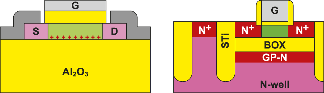
Figure 1. The venerable SOS MOSFET next to its FD-SOI offspring.
In the meantime, the SOS transistor (Fig. 1) revealed promising assets: simple processing, perfect dielectric isolation for latch-up elimination, drastically reduced leakage and parasitic capacitance, enhanced radiation hardness. However, it was long admitted that SOS was not the best option. In the late 70’s, its decline was precipitated by the rise of SIMOX (Separation by Implantation of Oxygen) technology.
II. The Renaissance
The synthesis of SIMOX wafers is brutal: deep implantation of enormous amounts of oxygen (≈ 2x1018 cm-2) to achieve a continuous buried oxide (BOX, Fig. 2a). Despite the astronomic number of dislocations and traps, Katsu Izumi and his team at NTT Labs succeeded in 1978 to fabricate improbable CMOS circuits.
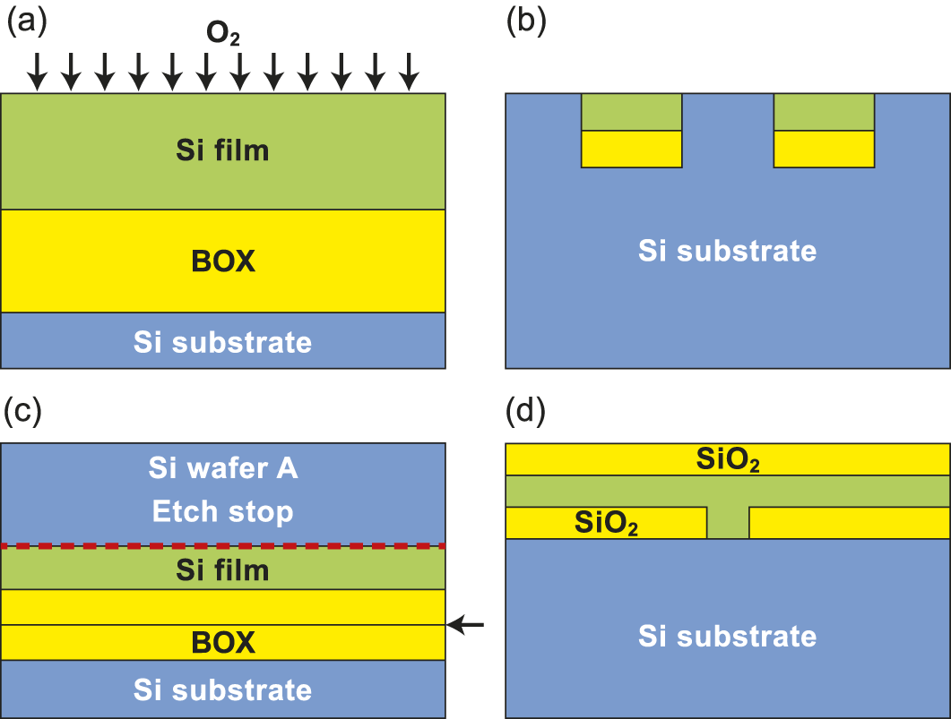
Figure 2. A few SOI variants: (a) SIMOX, (b) localized SOI (via SIMOX and SON), (c) wafer bonding, (d) CELO.
It was the presence of relatively thin Si film (200 nm) and BOX (400 nm) that opened the back gate: biasing the substrate enabled the tuning of the threshold voltage, a unique asset of fully-depleted SOI (FD-SOI) transistors. Any SOI device comprises an upside-down MOS structure where the BOX plays the role of gate dielectric. We showed that two probes acting as source and drain are sufficient to operate the pseudo-MOSFET (Ψ-MOSFET), the undisputable method for electrical characterization of SOI materials. This kind of embryonic transistor is what the Three Tenors at the Bell Labs attempted to prove 75 years ago. Since SOI was not imagined yet, they ended up with the bipolar transistor.
The performance of test CMOS circuits on SIMOX was incentive to pursue material developments and design dedicated ion implanters and furnaces. Peter Hemment organized a dynamic European Consortium in competition with American and Japanese organizations. IBIS Corporation brought SIMOX on the marketplace.
During his sabbatical at LETI, Yannis Stoemenos had the hot idea of annealing at extremely high temperature (>1300 °C). This cleared the silicon film of crystal defects leaving a sharp Si-SiO2 interface and a leakage-free BOX. SOITEC Company was founded by A-J. Auberton-Hervé and J-M. Lamure with the initial goal of commercializing this top-quality SIMOX.
SIMOX was handicapped by its long and costly processing, low throughput and rather rigid thickness of film and BOX. The ITOX variant was conceived by Izumi-san’s group to lower the implant dose and reduce the layer thickness below 100 nm.
Material magicians uncovered astonishing SOI structures to compete with SIMOX.
Wafer Bonding (WB or BESOI) consists in mating two wafers, at least one of which is oxidized (Fig. 2c). The bonded structure is thinned down by etching and grinding to reach the target thickness of the film. Etch-stop layers (SiGe, porous Si, junctions) are helpful but insufficient for achieving ultrathin layers. WB technology is dedicated to thick power devices and sensors.
Zone Melting Recrystallization (ZMR) starts with the deposition of a polycrystalline Si layer on an oxidized wafer. A heat source (lamps, lasers, beams) is scanned across the surface to erase the grain boundaries and associated defects. The limited extension of the monocrystalline islands is a frustrating issue.
Epitaxial Lateral Overgrowth (ELO) favors the epitaxy of single-crystal silicon through seed windows opened on the oxidized bulk-Si wafer. The growth proceeds laterally and vertically, which implies a thinning step. This inconvenience is eliminated with the CELO variant of tunnel epitaxy through a confined cavity (Fig. 2d). ELO is fit for 3D integration as it does not require post-growth recrystallization at high temperature.
Full Isolation by Porous Oxidized Silicon (FIPOS) makes use of selected P-doped regions in a N-type wafer which are converted into porous silicon by anodic reaction. Thanks to their huge surface-to-volume ratio, the porous regions are preferentially oxidized to form the BOX.
The 80’s was a glorious decade for material science and device physics. The annual IEEE International SOI Conference was not only the grand scene for creativity but also the arena of memorable fights between the gladiators of competing camps. Jerome Lasky, Witek Maszara, Ulrich Gösele and their colleagues pushed the progress in wafer bonding technology. Gerry Neudeck advanced ELO process and demonstrated double-layer SOI devices stacked on top of each other. Atsushi Ogura invented the CELO variant used nowadays to combine Ge, III-V and silicon heterointegration. Jean-Pierre Colinge at CNET and George Celler at Bell Labs were fanatics about ZMR before thinking better.
While bulk-Si CMOS continued its triumphal (and boring) march from node to node, SOI was around to entertain imagination and boost novel concepts, smart characterization techniques and beautiful or lousy devices.
The theory of gate coupling and threshold voltage modulation was elaborated by Jerry Fossum and Hyung-Kyu Lim 40 years ago. After completing his PhD, Lim returned home and could not stop before becoming the boss of Samsung.
An ultrathin SOI film behaves as a quantum well where carrier confinement and subband splitting takes place; Yasuhisa Omura alerted on the inevitable rise in threshold voltage. Dimitris Ioannou was busy with the transient floating-body effects. We revealed the principle of volume inversion which stipulates that in a thin body the mobile carriers are no longer confined at the interface. Jean-Pierre Colinge invented the gate-all-around (GAA) MOSFET omnipresent today in nanowire and nanosheet devices. A fascinating three-tier image processor was fabricated at Mitsubishi by Akasaka’s team via monolithic integration in 1987, too early for volume production. All these bright guys are very old or worse.
III. The Smart-Cut Reign
In early 90’s, too many SOI materials kept competing, which means that none was really convincing. The dilemma was fixed by Michel Bruel from LETI and his genius idea of Smart-Cut. The processing sequence (Fig. 3) consists in transferring a premium-quality silicon layer from wafer A to a passive wafer P. The magic of Smart-Cut is the ability to detach a nanometer-thick film from wafer A using hydrogen implantation as an atomic scalpel (ion cut). Hydrogen ions implanted in wafer A generate fine microcavities which result in a mechanically fragile planar zone. Annealing or a mechanical force is used to split the wafers along the hydrogen-weakened zone rather than at the original bonding interface. The microcracks act as a zipper, leaving a well-controlled Si film on wafer P. The SOI wafer undergoes surface polishing and annealing to strengthen the bonded interface. The silicon film retains the excellent crystal quality of the high-grade wafer A which is recycled repeatedly; according to the sausage theorem, a slice is cheaper than the whole sausage. The handle wafer serves as mechanical support and is less costly.
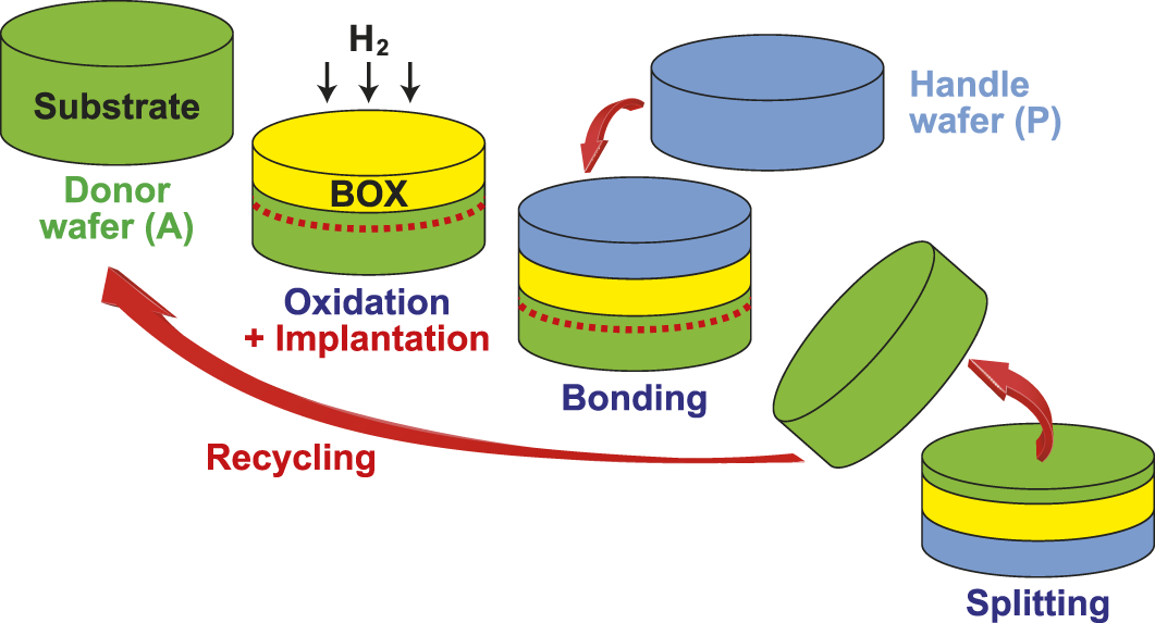
Figure 3. Synthesis of SOI wafer by Smart-Cut.
Smart-Cut technology provides a full range of thicknesses: Si film from 5 nm to 2 μm and BOX from 5 nm to 5 μm. 5 nm means 200,000 thinner than the initial thickness of the wafer. The film uniformity is amazing: ±4 Å´ across a 30-cm wafer is like travelling the world without seeing mountains taller than 4 cm. Low defectivity, sharp interfaces and high carrier mobility are other unrivalled assets.
The success of Smart-Cut can be inferred from collateral damage. First, the competition was killed, all other SOI materials left the arena. As of 2023, SOITEC and licensed companies provide the quasi-totality of FD-SOI wafers on the market. Second, in 30 years of sovereignty no new candidate could challenge Smart-Cut:
- Also based on wafer bonding, the Epitaxial Layer Transfer (ELTRAN) used a thin porous-Si buffer to define the splitting region. The Si film was grown directly on the porous template. Uniformity and throughput were fatal.
- Silicon-On-Nothing is Thomas Skotnicki’s SON. Sacrificial SiGe regions are grown on silicon wafer and receive a thin epitaxial Si layer. Selective etching of SiGe leaves cavities (the ‘nothing’ part of the SON) subsequently filled with oxide (localized SOI, Fig. 2b). SON could not comply with the variability criteria of billion-transistor chips but serves as a building brick for GAA nanowire and nanosheet MOSFETs.
- Silicon-On-Diamond for high-temperature circuits had a brief and innocent life.
Smart-Cut is a generic technology able to expand SOI to SOA (Something On Anything) where the mating materials defy the chemistry laws. Silicon can give way to more suitable semiconductors for speed (Ge, SiGe, InGaAs, strained layers), power (SiC by SmartSiC, GaN) or photonic devices. The faithful SiO2 BOX is replaceable by Al2O3, AlN and diamond for mitigating self-heating. Ferroelectrics or silicon nitride promote the BOX from a passive to an active role, enabling nonvolatile buried memory and universal memory.
RF-SOI is a success story originated from a seemingly insane idea of demolishing the quality of the BOX-substrate interface. The trap-rich SOI promoted by Jean-Pierre Raskin is actually a brilliant concept that conquered the RF market. Adding interface traps prevents the activation of a parasitic channel by BOX charges, and preserves the high resistivity of the substrate.
Two recent applications of Smart-Cut attract attention: (i) Piezoelectric-On-Insulator (POI) comprising a LiTaO3 film on high-resistivity substrate and (ii) transfer of layers containing pre-processed circuits from a silicon wafer to another substrate (3D integration, RF devices). Albeit Smart-Cut encouraged new materials to bond together, the divorce of the old couple, silicon and silicon-oxide, is seemingly impossible. Figure 4 summarizes the SOI story over the past 60 years.
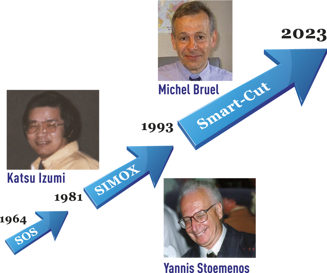
Figure 4. 60 years of SOI.
IV. SOI Transistors
Partially-depleted (PD) MOSFETs won the first set but finally lost the game against their fully-depleted (FD) cousins. Ghavan Shahidi pushed at IBM the adoption of PD-SOI for performance/power/area advantages over bulk-Si CMOS. Lower power for equivalent performance, or higher speed at same biasing were solid arguments. PD-SOI processors became available on the marketplace in 1995. AMD and Global Foundries followed in 2001 with high-end power-PC micro-processors. This route could not continue indefinitely for the limits of downscaling are similar in PD-SOI and bulk-Si MOSFETs whereas fully-depleted devices are well] equipped. Electrostatic considerations led Konrad Young define an intrinsic length, function of film thickness. A thumb-rule stipulates that a Si layer of thickness tsi can accommodate FD-SOI MOSFETs with a minimum length of L = 4tsi. Smart-Cut enabled thinner and shorter transistors. Imagine a cargo crossing an ocean just a few meters deep. Without waves or tsunamis, the cargo moves faster with reduced consumption. This is exactly what happens in ultrathin SOI transistors where the electrons are more mobile and most parasitic effects are suppressed.
A peculiar short-channel effect in FD-SOI transistor is the penetration of the electric field from source and drain into the body via the BOX. The fringing field reduces the threshold voltage and contributes to DIBL (drain-induced barrier lowering). This is why a thin BOX (< 20 nm) is unavoidable for further downscaling.
A state-of-the-art FD-SOI transistor (Fig. 1b) features 6 nm film and 20 nm BOX. The body is undoped and there is no need of halos, pockets or LDD regions. A highly-doped ground-plane underneath the BOX serves as back gate. The source and drain are raised by epitaxial regrowth with in-situ doping to minimize the series resistance. Each transistor is isolated from the next one by STI. 90% of the process modules, including the gate stack, are imported from bulk-Si CMOS. The duplication of such a transistor by sort of copy-and-paste process is the foundation of the monolithic integration of 3D circuits.
Around the turn of the millennium, many research groups joined the SOI family. Francisco Gamiz developed Monte-Carlo-in-Granada simulations, in competition with his dear friends from Udine (Luca Selmi and David Esseni). Ron Schrimpf and colleagues in Vanderbilt focused on the permanent effects of cumulated radiation dose. Gérard Ghibaudo (Grenoble), Babis Dimitriadis (Thessaloniki) and Cor Claeys (IMEC) enriched knowledge in noise and specialized characterization methods. Joao-Antonio Martino built an enthusiastic team at the University of São Paulo. Outstanding contributions came from the groups led by Shinichi Takagi and Toshiro Hiramoto at the University of Tokyo, by Jong-Ho Lee at Seoul National University, and by Tamara Rudenko at the Academy of Science in Ukraine. How can I list all who would deserve it?
Stunning device concepts fueled by FD-SOI came out since 2010. Colinge invented the junctionless MOSFET with mandatory ultrathin body. We demonstrated the four-gate MOS transistor, where each gate can independently turn on and off the current. A number of capacitorless DRAM variants use the MOSFET to store and read information. Band-modulation devices, electrostatic doping and tunneling FETs all take advantage of ultrathin SOI films.
Inspired from several SOI workshops organized in Grenoble, the annual EuroSOI conference has formally been initiated 20 years ago in Granada. It is sponsored by IEEE and travels around Europe, attracting specialists from all continents. Alexei Nazarov organized sister SOI workshops in Ukraine. Carlos Mazuré, aided by Bich-Yen Nguyen and Ionut Radu, put together the SOI Industry Consortium where designers and technologists have started to talk to each other.
Global Foundries, IBM, STMicroelectronics and some Japanese sumos acquired expertise and ambitions in FD-SOI circuits. Technology modules, models and design libraries were elaborated to conquer the market. Everyone expected FD-SOI to replace the dying bulk-Si CMOS before 2010. Conservative management delayed the switch, letting Intel to make a big surprise by introducing their FinFETs, soon adopted by major companies. This is how FD-SOI missed the chance to be a premier technology.
However, SOI did not give up and today the market is booming. It is the technology for low-power, IOT and AI circuits, RF and reconfigurable devices. Many emerging devices wouldn’t have been discovered had SOI not been around. Band-modulation and electrostatic doping are powerful concepts unknown 20 years ago.
V. Special Mechanisms in FD-SOI MOSFET
An FD-SOI transistor is a perfectly isolated nano-box which accommodates unusual effects our dear 75-year-old MOS patriarch never heard of. The following is a homeopathic introduction.
Interface Coupling–The properties of one channel depend on the quality and biasing of the opposite interface. The primary application is the tuning of the threshold voltage VT via the back gate. For 200 mV shift in VT the OFF current and standby power are reduced by three orders of magnitude. Only FD-SOI transistors can enjoy this capability which is instrumental in low-voltage, low-power circuits.
Supercoupling–The coexistence of electron and hole channels facing each other is denied in films thinner than 10 nm. Supercoupling inhibits the floating-body effects but causes bilayer devices (single-transistor DRAM and TFET) to fail.
Electrostatic Doping–Volume inversion and accumulation enable the carrier spreading in the whole body. Such gate-induced doping behaves in many respects as a chemical doping with the additional merit of reconfigurability. The possibility to emulate P-N junctions in a fully-depleted body just by adding gates has fascinating applications (virtual diode, undoped Esaki diode, band-modulation devices).
Thickness Effects–The carrier mobility is hardly affected by film thinning. Only below 3 nm does the mobility drop due to surface roughness. The energy quantization induces interesting transport and electrostatic properties.
VI. Next
Nanoelectronic devices have more impact on our society than politics and religions. Whether this is wonderful or devastating does not really matter; progress is ineluctable to satisfy the exponential demand. However, challenges are tough at several levels: technological, financial, societal and even geopolitical.
Nobody could predict, 60 years ago, the adventurous story of SOI technology. I believed in SOI for almost 50 years, a few more will not hurt. There is no doubt that SOI will be there for the celebration of the 150th anniversary of the transistor.
-----------------
Acknowledgements. An enriched version of this article will appear on the commemorative volume, 75th Anniversary of the Transistor, IEEE Press-Wiley, 2023. Details and references are also available in recent books:
References
J-P. Colinge, “Silicon-on-Insulator Technology: Materials to VLSI,” 3rd ed., Springer, 2004.
J.G. Fossum, V.P. Trivedi, “Fundamentals of Ultra-Thin-Body MOSFETs and FinFETs,” Cambridge Univ. Press, New York, USA, 2013.
S. Cristoloveanu. “Fully depleted silicon–on–insulator,” Amsterdam, Elsevier, 2021.
1 S. Cristoloveanu is Emeritus Director of Research CNRS at IMEP-LAHC laboratory of the Polytechnic Institute of Grenoble, France. (e-mail: sorin.cristoloveanu@grenoble-inp.fr).
Evolution of Surface-Potential-Based Compact Modeling
M. Miura-Mattausch, T. Iizuka, H. Kikuchihara, H. J. Mattausch, and S. Saha
Conventionally, a compact model of an electronic device is developed for utilization in circuit simulation. This means that the main task of the compact model is to accurately describe the characteristics of a device as a function of the applied voltages by simple equations in order to predict the performance of circuits using this device with sufficient precision. This overview article focuses on the compact modeling of the metal-oxide-semiconductor field-effect transistor (MOSFET)-device structure, which has the largest variety of applications. However, the modeling methodology is valid for any type of transistor or electronic device.
Shortly after the transistor invention, Shockley developed the well-known pn junction current-voltage equation [1]. The underlying physics and assumptions can be found in most semiconductor textbooks (e.g. [2]), describing the control of the current by an applied bias. The electrostatics of the pn junction is characterized by the Poisson equation, which describes the relationship between the potential distribution and the charges within the pn junction (see Fig. 1). Based on the Poisson and continuity equations for electrons and holes, with appropriate boundary conditions, the current-voltage relationship can be obtained.
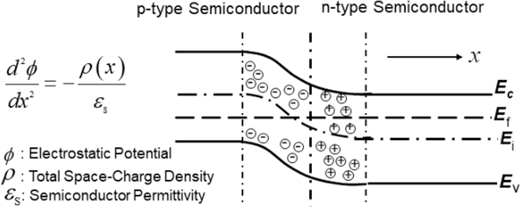
Figure 1. Potential distribution along the p/n junction as the solution of the Poisson equation.
Shockley’s modeling concept has been extended to MOSFET devices by Pao and Sah in 1966 [3]. Aside from using a gate voltage (Vgs) induced electric field to control the current in a direction perpendicular to the field, known as the field effect [4], the main difference is that the carriers in the MOSFET are confined within a potential well at and near the semiconductor surface. The drain voltage (Vds) is applied to enable the carrier flow into the drain from the source according to the potential gradient (see Fig. 2). Pao & Sah solved the Poisson equation in two dimensions, the well depth direction x and the channel direction y. Consequently, the solution of the Poisson equation is reduced into a two-dimensional (2D) potential distribution. Previously, Sah has focused only on the strong-inversion condition, where the potential distribution along the channel can be drastically simplified, and derived a simple analytical equation for the drain current Ids as [5]
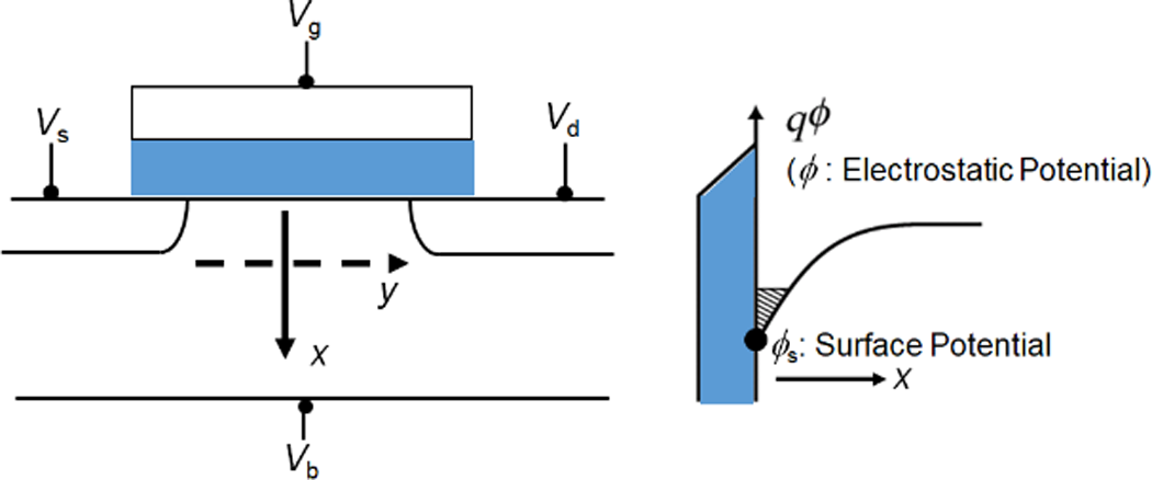
Figure 2. MOSFET structure schematic together with the potential φ distribution in the x direction.
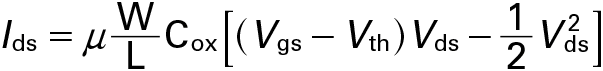 |
(1) |
Here, μ is the carrier mobility and the threshold voltage Vth is the Vgs value needed to form the channel at the onset of strong inversion. This equation was commonly used in compact analytical modeling of MOSFETs for circuit simulation.
1. Circuit-Simulation Model
The equivalent-circuit model for the MOSFET, developed by Meyer, is shown in Fig. 3 in a simple way [6]. A compact model provides equations for all elements in the equivalent circuit model. The current is an integration of the carrier density multiplied by velocity from source to drain. The capacitances are the derivatives of charges induced on the transistor nodes (Vs, Vg, Vd, and Vb). As the current equation, the Sah equation is taken and the analytical charge equations are derived in the same manner as Ids. Equations for subthreshold and saturation conditions are written phenomenologically to enable the completion of the switching-performance simulation.
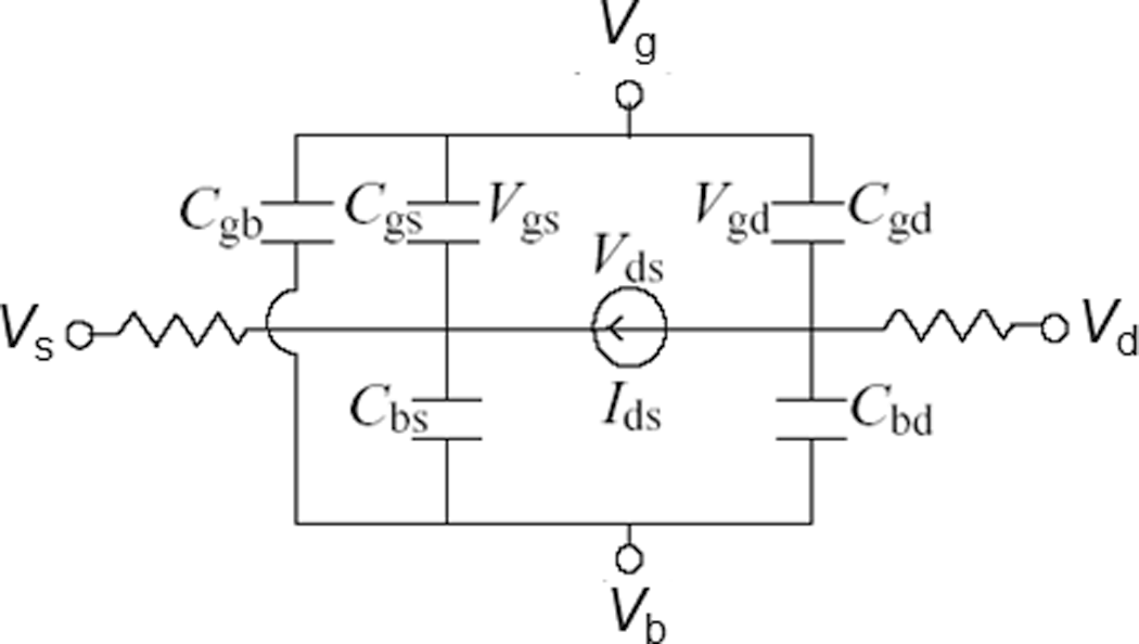
Figure 3. Equivalent MOSFET circuit proposed by Meyer.
The basic transistor equations are derived on the basis of the Maxwell equations, where the potential φ is a function of position within the transistor. Instead of solving the Poisson equation, the potential values at the source and drain side are fixed to φ = 2ΦB and φ = 2ΦB +Vds, respectively, where ΦB = kT/q ln(Nsub/ni) [5]. Since the SPICE (Simulation Program with Integrated Circuit Emphasis) circuit simulator was developed at UC Berkeley in an early stage during the 1970s and provided for public usage [7], circuit simulation has become a powerful method for circuit development.
2. Vth-Based Compact Model
The Vth-based model development was completed as BSIM4 [8] at the beginning of this millennium under the support of the CMC (Compact Model Council) [9], and has been widely used for circuit design. Singularities in modeled derivatives of device characteristics, caused by the piece-wise modeling approach, have been removed by smoothing functions. Thereafter, the Vth-based modeling method became the mainstream in the compact-modeling community. However, shortcomings of the applied simplifications, considering the strong-inversion condition, became obvious as technology advanced further. Subthreshold characteristics give rise to important technological features that must be considered. Thus, to have a physics-based analytical model for the subthreshold region, as well as a smooth continuous transition to the strong-inversion region, became essential. Due to the parameters introduced through smoothing functions, the connection between the model parameters and the measured device parameters became more tenuous, necessitating further improvements in the modeling approach.
3. Surface-Potential-Based Compact Model
In the 1970s, since CMOS technology became ready for circuit applications with low power [10], the development of large-scale integrated circuits became the mainstream. Further, the transistor-size reduction was accompanied by a bias reduction, requiring good Vth control. Here, the importance of the Poisson equation-based modeling has been raised again due to its validity for all bias conditions and its physical correctness. Three investigations have been published nearly at the same time [11], [12], [13]. The main improvement was the introduction of the charge-sheet approximation [11], which reduces the Pao-Sah’s double integrals into one, only in the channel direction, while neglecting the carrier density variation in the channel-depth direction, since the space-charge density variation in that direction is negligible in comparison to that along the channel length. Thus, only the surface-potential distribution along the channel is considered. The short-channel effect, accompanying the size reduction, was the next phenomenon to be modeled. This has been done by considering the lateral electric field in the Poisson equation analytically [14]. The first complete model for advanced technologies was developed at Siemens in the early 1990s, which then has been further developed and named HiSIM [15]. This model solves the Poisson equation iteratively to avoid any approximations with a good initial guess and preserves the smoothness of the higher-order derivatives of physical quantities. The Poisson equation is solved only two (2) times (at the source side and at the drain side) for describing potential distribution within the transistor. The calculated potential values are used to determine all charges and currents induced within the semiconductor. It has been demonstrated that the circuit simulation time could be even reduced with a simplified source code due to the simple model description. A big advantage of potential-based modeling is that the meaning of most model parameters coincides with corresponding technological device parameters. The predictability of the HiSIM compact model is demonstrated in Fig. 4 [16].
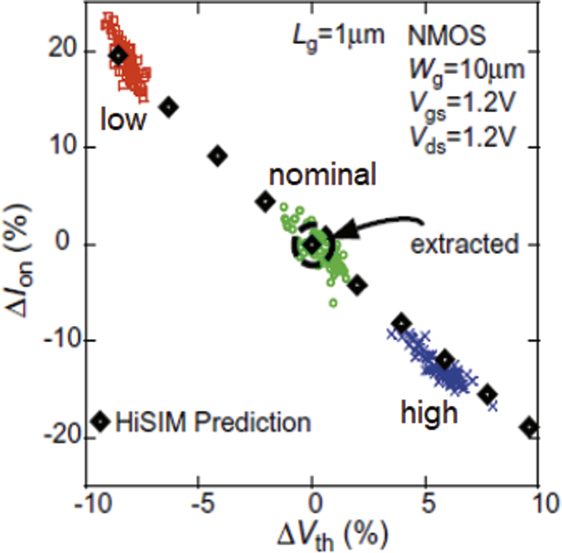
Figure 4. Reliability test of the developed model for three different wafers with different impurity concentrations, where only the nominal-device data has been used for the model, and only the impurity concentration was changed for low and high cases. Black diamonds are the model predictions.
A major challenge was to develop a thin-layer MOSFET model for devices composed of different layers, where not only the surface potential but the entire potential distribution within different layers must be solved (see Fig. 5 [17]). It has been demonstrated that compact modeling by solving the Poisson equation iteratively is suitable even for such cases as MG-MOSFETs and GAA-MOSFETs, e. g. [18]. Due to the CMC leadership, the movement of compact models from Vth-based to potential-based modeling has been accelerated, though the mainstream of potential-based modeling is still using analytical solutions of the Poisson equation [19]. However, it has been slowly accepted, that deriving an analytical description for calculating the potential values requires several simplifications, which may bring problems for accurate modeling of advanced technologies.
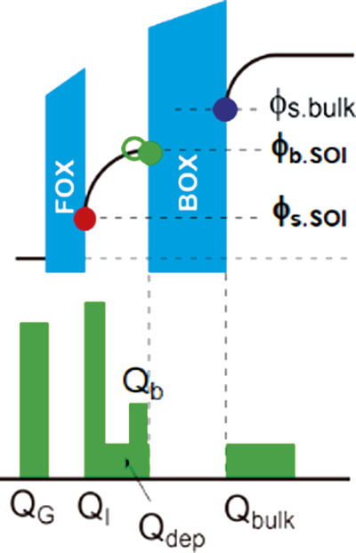
Figure 5. Schematic of thin-layer MOSFET and its potential distribution vertical to the surface.
3.1. NQS Effect
In the beginning of the 1990s, internet technology (IT) development emerged throughout the world, requiring high-speed MOSFETs to realize monolithic integration of different circuit functions. The carrier transit delay with respect to bias changes limits the transistor’s cut-off frequency (fT) improvement [20]. Therefore, a new task was to model the carrier-transit-delay effect, which is basically determined by the carrier mobility. During switching on and -off, carriers don’t appear and disappear immediately along with the switching waveform. This phenomenon is called the Non-Quasi-Static (NQS) effect caused by the carrier-transit delay (see Fig. 6 [21]). Resistances and capacitances induced within a transistor influence this delay too. Therefore, the delay has been modeled originally by dividing the channel into several segments and by stacking resistances between these segments, as shown in Fig. 7 [22]. However, such a modeling approach increases circuit simulation time drastically. A more reasonable approach considers the carrier-transit time, which is required to complete the movement within the transistor, explicitly. If the transit time is longer than the switching time, only a part of the carriers can complete this action [23]. Thus, a reduced amount of charge is considered in the Poisson equation, resulting in a reduction of the potential values at the same bias condition. The resulting NQS model for RF performances has been verified with measurements, as shown in Fig. 8 [24].
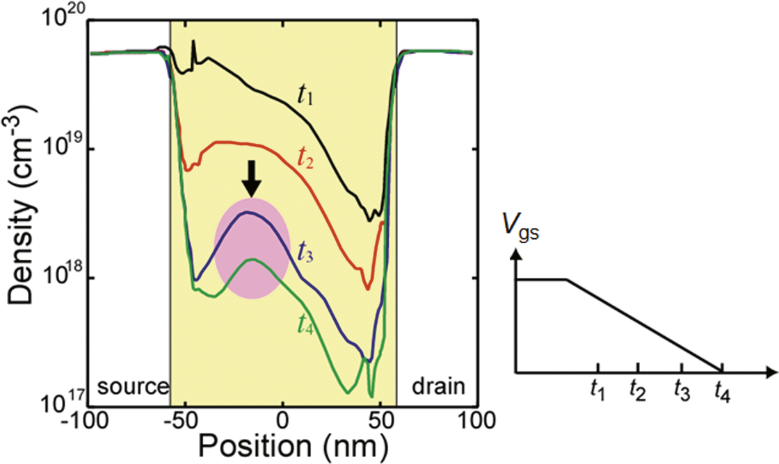
Figure 6. 2D numerical device simulation of the carrier-density distribution within the MOSFET channel. The transit delay is obvious in the middle of the channel.
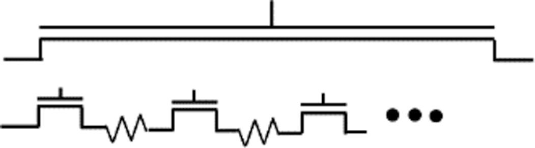
Figure 7. Elmore channel-segmentation model for the carrier-transit delay.
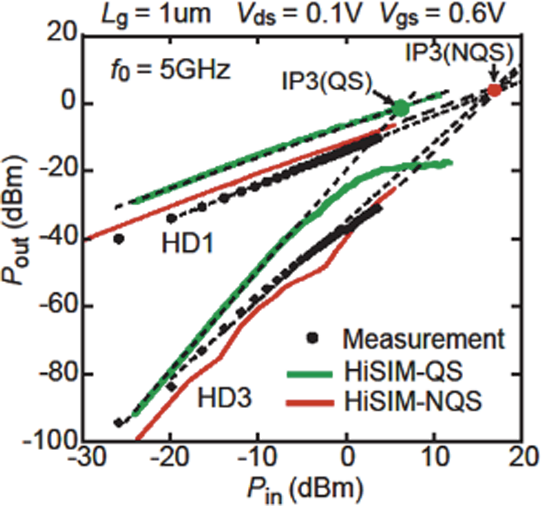
Figure 8. HiSIM-model-calculation results for harmonic distortions with/without the NQS effect in comparison to measurements.
3.2. High-voltage (HV) Modeling with an Internal Node
The MOSFET has been extended for high-voltage (HV) applications by introducing long resistive drift regions to sustain the applied high voltage (see Fig. 9) [25]. In the early stage of the compact model development, HV-MOSFET models consisted of a conventional MOSFET and a resistance, called a macro-model. The disadvantage of this modeling approach is the complication of the model parameter extraction. And, instability in circuit simulation has also been reported. Thus, a new modeling approach has been proposed by introducing an internal node explicitly between the intrinsic MOSFET and the resistive drift region [26]. The potential distribution is solved from the source to the internal node and from the internal node to the drain contact by a circuit simulator. The calculated results of the potential characteristics are depicted together in Fig. 9.
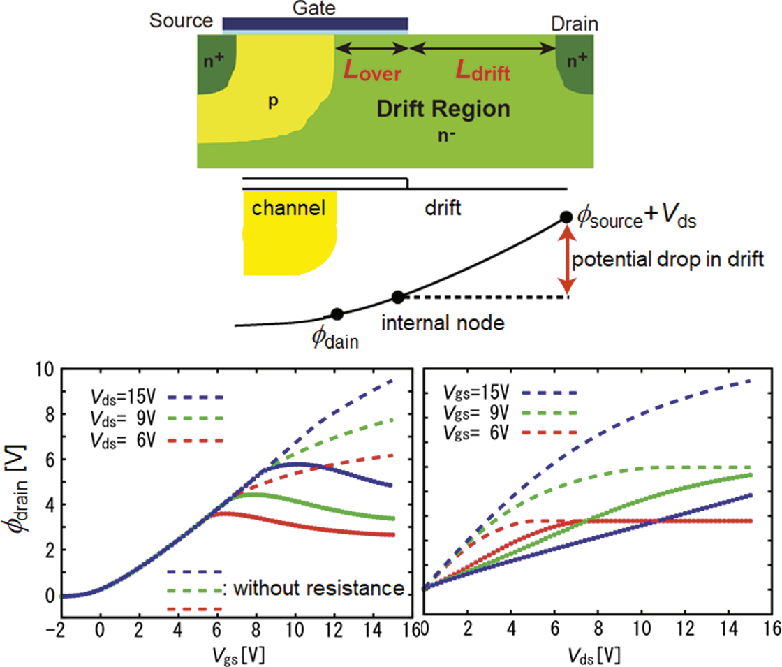
Figure 9. Schematic of a high-voltage MOSFET (LDMOS) (top) and its potential distribution (middle) together with potential values with (bottom left) / without (bottom right) the drift-resistance contribution.
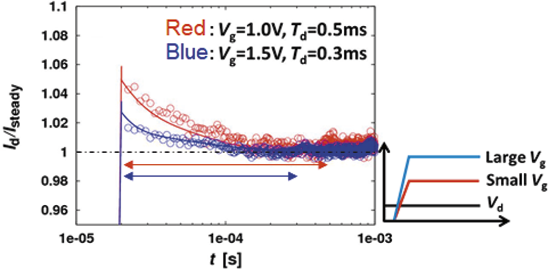
Figure 10. Measured trapping-time constant Td from switching-on characteristics under two different bias conditions.
HV-MOSFETs have been realized not only by introducing a long resistive region but also by structural modifications such as planar or trench structures. By combining a MOSFET with a bipolar transistor, the IGBT has been invented [27], which has realized bias ranges up to a thousand volts even with Si-based technologies. The main modeling difficulty is that the potential drop, induced within the overlapping region of the MOSFETs drift region and the bipolar base, is strongly influenced by the IGBT structure and the bias conditions. It has been demonstrated that consistent and accurate compact modeling is possible by introducing an additional internal node, which is solved iteratively again by the circuit simulator [28]. Thus, compact modeling is entering into a new era, getting more freedom with the use of internal nodes, solved by a circuit simulator. Self-heating-effect models are also a mandatory requirement for power devices.
3.3. Trap Model
The Poisson equation includes all charges induced within the semiconductor, and thus the entire potential distribution along the transistor depth direction is required to calculate charges. Trap charges can be induced during circuit operation as well as device fabrication. Carriers are trapped/detrapped by crystal defects mostly at the insulator/semiconductor interface. A trap increase is known as the origin of circuit degradation [29]. The physical quantity, determining the easiness of carriers to be trapped, is the capture cross section σ. In compact modeling, σ is macroscopically modeled by the time constant Td, which is written with σ as follows [30]
 |
(2) |
n: Carrier Density |
σ: Capture Cross Section |
vth,n: Thermal Velocity |
A: Trapping Coefficient |
4. Compact Model vs. TCAD
The first technology CAD program (called TCAD by Dutton [31]) was developed by Scharfetter and Gummel [32] in 1969. The breakthrough invention was the discretization within the device to solve the potential distribution numerically. The concept has been further developed to solve the basic equations numerically in two dimensions (x and y) or even in three dimensions (x, y, and z). Instead of solving numerically, a compact model derives simplified equations by integrating the distribution from source to drain, to obtain quantities suitable for compact models at transistor nodes. Macroscopic quantities, mainly obtained from measurements, reflect the node potential conditions. Predicting the switching performance accurately is not an easy task, because characteristics of a real transistor demonstrate many discrepancies compared with the compact model of the ideal device. By investigating the target circuit, however, model deficits, which prevent from an accurate circuit-performance prediction, become often clear. For such a deficit case, a TCAD investigation is carried out to find the underlying reason. Since the basic equations are the same for the two methods of TCAD and compact modeling, the model parameter dependencies of the device characteristics must preserve those of the TCAD results.
5. Verilog-A Language
The compact-model equations must be implemented in the circuit simulator, which should provide an interface for this purpose. At an early stage of the model development, nevertheless, this implementation was a tough task for the model developers. The Verilog-A language has been originally developed for analog circuit designers to verify or design their own analog model equations to achieve their specific modeling tasks. In parallel, the Verilog-A language has been extended for compact-model developers as an alternative language to C-Code [33]. A big advantage of the Verilog-A code is that derivatives are numerically solved within the simulators. The Verilog-A description has been further extended for compact-model developers to support the easy implementation of quite complicated model constructions into commercial circuit simulators, providing model developers with more freedom in their development framework. Additionally, new solution-algorithm developments of circuit simulators have improved drastically the simulation time as well as the model calculation stability.
6. Circuit Design Perspectives
On the circuit level, the compact models have mainly two application areas. The first is the design of analog and RF circuits. The second is the development of elementary digital circuit cells and macro-circuit blocks for industrial design libraries, which are then used by higher-level design and verification software, to compose the complete circuits for different application tasks [34]. The preserved physical relationships between the actual device parameters and the parameters of potential-based models allow the circuit designers to better understand the effects of technology changes on the performance characteristics of the designed circuits. It further facilitates the simulation of statistical technology variations and aging effects on their designed circuits. Even though the simulation speed remains a major consideration for the characterization of the design-library cells, it is the model accuracy, which has become the most important for both analog and digital circuit design. In particular for advanced technologies, with device-structure sizes reaching below 10 nm, simple digital cells such as inverters or 2-input logical cells start to show strong analog features, requiring accurate compact models for more accurate characterization. The surface-potential compact models now have run-time speeds comparable to Vth-based models [35], so that they have become the mainstream in compact-model development and practical applications [9].
7. Summary
The development of the compact modeling approach, based on the potential distribution induced within a transistor, is reviewed. The purpose of a compact model is to describe the transistor characteristics in a simple but accurate way, to enable correct circuit-performance prediction. Therefore, the basic physics of observed phenomena must be modeled by simplified and yet physically correct equations. To meet such requirements, potential-based modeling is a natural fit. A compact model and TCAD are both based on the same transistor equations. The difference is that TCAD considers the distribution of all physical quantities within a device, and a compact model integrates these distributions to calculate transistor characteristics at its nodes. The shortcomings of resulting simplifications, introduced for analytical integration, can be examined using TCAD, to identify observed phenomena still missing in the compact modeling. In this way, compact modeling is performed by learning from measurements macroscopically and from TCAD microscopically.
References
[1] W. Shockley, “The theory of p-n Junction in Semiconductors and p-n Junction Transistor,” Bell Syst. Tech. J., 28, 435, 1949.
[2] S. M. Sze, “Physics of Semiconductor Device (Second Edition)”, New York, John Wiley & Sons, Inc., 1981.
[3] H. C. Pao and C. T. Sah, “Effects of diffusion current on characteristics of metal-oxide (insulator)-semiconductor transistors,” Solid-State Electron., vol. 9, no. 10, pp. 927–937, 1966.
[4] J. E. Lilienfeld, “Method and apparatus for controlling electric currents,” filed in Oct. 8, 1926 and US patented Jan. 28, 1930.
[5] C. T. Sah, “Characteristics of the metal-oxide-semiconductor transistors,” IEEE Trans. Electron Devices, vol. ED-11, no. 7, pp. 324-345, 1964.
[6] J. E. Meyer, “MOS models and circuit simulation,” RCA Rev., vol. 32, pp. 42-63, March, 1971; J. E. Meyer, “Computer-Aided MOS/SOS Design,” Proc. Computer-Aided System Design Seminar, Cambridge, Mass., April 1969.
[7] L. W. Nagel and D. O. Pederson, “Simulation program with integrated circuit emphasis (SPICE),” Proc. 16th Midwest Symp. on Circuit Theory, Waterloo, April 1971; L. W. Nagel and D. O. Pederson, “SPICE (Simulation Program with Integrated Circuit Emphasis), “Memorandum No. ERL-M382, University of California, Berkeley, Apr. 1973: http://www.eecs.berkeley.edu/Pubs/TechRpts/1973/22871.html.
[8] BSIM4.0.0 MOSFET Model, User’s Manual, Department of Electrical Engineering and Computer Science, University of California, Berkeley CA, 2000; http://bsim.berkeley.edu/models/bsim4/.
[9] CMC-Compact Model Council: https://web.archive.org/web/20110511071827/
http://www.geia.org/index.asp?bid=597; CMC-Compact Model Coalition: https://si2.org/cmc/.
[10] Y. Suzuki, M. Hirasawa, and K. Odagawa, “Clocked CMOS calculator circuitry,” 1973 IEEE Int. Solid-State Circuits Conf. Digest of Technical Papers, Philadelphia, PA, USA, 1973, pp. 58-59.
[11] J. R. Brews, “A Charge-sheet model of the MOSFET,” Solid-State Electron., vol. 21, pp.345-355, 1978.
[12] G. Baccarani, M. Rudan, G. Spadini, “Analytical i.g.f.e.t. model including drift and diffusion currents,” IEE J. Solid-State and Electron Devices, vol. 2, no.2, pp. 62-68, 1978.
[13] F. Van der Wiele, “A long–channel MOSFET model,” Solid-State Electron., vol. 22, no.12, pp. 991-997, 1979.
[14] M. Miura-Mattausch and H. Jacobs, “Analytical model for circuit simulation with quarter micron metal oxide semiconductor field effect transistors: Subthreshold characteristics,” Jpn. J. Appl. Phys., vol. 29, no. 12, pp. L2279–L2282, 1990; M. Miura-Mattausch, H. J. Mattausch, and T. Ezaki, “The physics and modeling of MOSFETs,” World Scientific, 2008.
[15] M. Miura-Mattausch, U. Feldmann, A. Rahm, M. Bollu, and D. Savignac, “Unified complete MOSFET model for analysis of digital and analog circuits,” IEEE Trans. CAD/ICAS, vol. 15, no. 1, pp. 1–7, 1996; M. Suetake, K. Suematsu, H. Nagakura, M. Miura-Mattausch, and H.J. Mattausch, “HiSIM: A Drift-Diffusion-Based Advanced MOSFET Model for Circuit Simulation with Easy Parameter Extraction,” Proc. 2000 Int. Conf. Simulation of Semicon. Processes and Devices, pp. 261-264, Seattle, 2000.
[16] N. Sadachika, S. Mimura, A. Yumisaki, K. Johguchi, A. Kaya, M. Miura-Mattausch, H. J. Mattausch, “Prediction of Circuit-Performance Variations from Technology Variations for Reliable 100 nm SOC Circuit Design”, IEICE Trans. Electronics, Vol. E94-C, No. 3, pp. 361-367, Tokyo, 2011.
[17] N. Sadachika, D. Kitamaru, Y. Uetsuji, D. Navarro, M. M. Yusoff, T. Ezaki, H. J. Mattausch, M. Miura-Mattausch, “Completely Surface-Potential-Based Compact Model of the Fully Depleted SOI-MOSFET Including Short-Channel Effects,” IEEE Trans. Electron Devices, Vol. 53, No. 9, pp. 2017-2024, 2006; M. Miura-Mattausch, U. Feldmann, Y. Fukunaga, M. Miyake, H. Kikuchihara, F. Ueno, H. J. Mattausch, T. Nakagawa, and N. Sugii, “Compact modeling of SOI MOSFETs With Ultrathin Silicon and BOX Layers,” IEEE Trans. Electron Devices, Vol. 61, No. 2, pp. 255-265, 2014.
[18] F. Avila Herrera, Y. Hirano, T. Iizuka, M. Miura-Mattausch, H. Kikuchihara, D. Navarro, H.J. Mattausch, and A. Ito, “Leading-Edge Thin-Layer MOSFET-Potential Modeling Toward Short-Channel-Effect Suppression and Device Optimization”, IEEE J. Electron Devices Society, Vol. 7, pp. 1293-1301, 2019.
[19] G. Gildenblat, D. B. Klaassen, R. van Langevalde, X. Li, A. J. Scholten, G. D. J. Smit, H. Wang, W. Wu, “PSP: An Advanced Surface-Potential-Based MOSFET Model for Circuit Simulation,” IEEE Trans. Electron Devices, Vol. 53, No. 9, pp. 1979-1993, 2006.
[20] Y. P. Tsividis, “Operation and Modeling of the MOS Transistor,” McGraw-Hill, 1999.
[21] T. Okagaki, M. Tanaka, H. Ueno, and M. Miura-Mattausch, “Importance of Ballistic Carriers for the Dynamic Response in Sub-100nm MOSFETs,” IEEE Electron Device Letters, Vol. 23, No. 3, pp. 154-156, 2002.
[22] W. C. Elmore, “The transient response of damped linear networks with particular regard to wideband amplifiers,” J. Appl. Phys., Vol. 19, No.1, pp. 55–63, 1948.
[23] N. Nakayama, D. Navarro, M. Tanaka, H. Ueno, M. Miura-Mattausch, H. J. Mattausch, T. Ohguro, S. Kumashiro, M. Taguchi, and S. Miyamoto, “Non-quasi-static model for MOSFET based on carrier transit delay,” Electronics Letters, Vol. 40, No. 4, pp. 276–278, 2004; D. Navarro, Y. Takeda, M. Miyake, N. Nakayama, K. Machida, T. Ezaki, H. J. Mattausch, M. Miura-Mattausch, “A carrier-Transit-Delay-Based Nonquasi-Static MOSFET Model for Circuit Simulation and Its Application Harmonic Distortion Analysis,” IEEE Trans. Electron Devices, Vol. 53, No. 9, pp. 2025-2034, 2006.
[24] Y. Takeda, D. Navarro, S. Chiba, M. Miura-Mattausch, H. J. Mattausch, T. Ohguro, T. Iizuka, M. Taguchi, S. Kumashiro, and S. Miyamoto, “MOSFET Harmonic Distortion Analysis up to the Non-Quasi-Static Frequency Regime,” IEEE 2005 CICC, pp. 827-830, San Jose, 2005.
[25] B. J. Baliga, “Silicon RF power MOSFETs,” World Scientific, 2005.
[26] H. J. Mattausch, M. Miyake, T. Iizuka, H. Kikuchihara, M. Miura-Mattausch, “The Second-Generation of HiSIM_HV Compact Models for High-Voltage MOSFETs”, IEEE Trans. Electron Devices, Vol. 60, No. 2, pp. 653-661, 2013; https://www.hisim.hiroshima-u.ac.jp/cgi/HiSIM_HV/public_release.cgi.
[27] B. J. Baliga, “Fundamentals of Power Semiconductor Devices,” Springer Science, 2008; R. Kraus and H.J. Mattausch, “Status and Trends of Power Semiconductor Device Models for Circuit Simulation”, IEEE Trans. Power Electronics, Vol. 13, No. 3, pp. 452-465, 1998.
[28] A. Tone, Y. Miyaoku, M. Miura-Mattausch, H. Kikuchihara, U. Feldmann, T. Saito, T. Mizoguchi, Y. Yamamoto, and H.J. Mattausch, “HiSIM_IGBT2: Modeling of the dynamically varying balance between MOSFET and BJT contributions during switching operations”, IEEE Trans. Electron Devices Vol. 66, No. 8, pp. 3265-3272, 2019.
[29] T. Grasser, H. Reisinger, P. J. Wagner, B. Kaczer, “Time dependent defect spectroscopy for characterization of border traps in metal-oxide-semiconductor transistors,” Phys. Review B, vol. 82, no. 245318, 2010; H. Tanoue, A. Tanaka, Y. Oodate, T. Nakahagi, D. Sugiyama, C. Ma, H. J. Mattausch, and M. Miura-Mattausch, “Compact modeling of dynamic MOSFET0degradation due to hot-electrons,” IEEE Trans. Device and Materials Reliability, Vol. 17, No. 1, pp. 52-58, 2017.
[30] Y. Oodate, Y. Tanimoto, H. Tanoue, H. Kikuchihara, H. J. Mattausch, and M. Miura-Mattausch, “Compact modeling of the transient carrier trap/detrap characteristics in polysilicon TFTs,” IEEE Trans. Electron Devices, Vol. 62, No. 3, pp. 862-868, 2015.
[31] R. W. Dutton, “Modeling and simulation for VLSI,” 1986 Int. Electron Devices Meeting, Los Angeles, CA, USA, 1986, pp. 2-7.
[32] D. L. Scharfetter and H. K. Gummel, “Large signal analysis of a silicon read diode oscillator,” IEEE Trans. Electron Devices, Vol. 16, No. 1, pp. 64-77, 1969.
[33] G. Coram, “How to (and how not to) write a compact model in Verilog-A,” in Proc. 2004 IEEE Int. Behavioral Modeling and Simulation Conference, BMAS 2004, , San Jose, CA, USA, pp. 97-106; G. Coram and C. McAndrew, “Verilog-A for compact modeling: Best practices for high quality model authoring,” in 2005 Workshop on Compact Modeling for RF/Microwave Applications (CMRF 2005), Santa Barbara, CA, USA, Oct. 12, 2005.
[34] C. Bhargava and G. M. Khanal, “Advanced VLSI Technology: Technical Questions and Solutions,” River Publishers, 2020.
[35] H.J. Mattausch, M. Miyake, T. Yoshida, S. Hazama, D. Navarro, N. Sadachika, T. Ezaki, and M. Miura-Mattausch, “HiSIM2 Circuit Simulation: Solving the Speed versus Accuracy Crisis,” IEEE Circuits and Devices Magazine, Vol. 22, No. 9, pp. 29-38, 2006.